Datasheet Details
| Part number | K2111 |
|---|---|
| Manufacturer | Kexin |
| File Size | 42.25 KB |
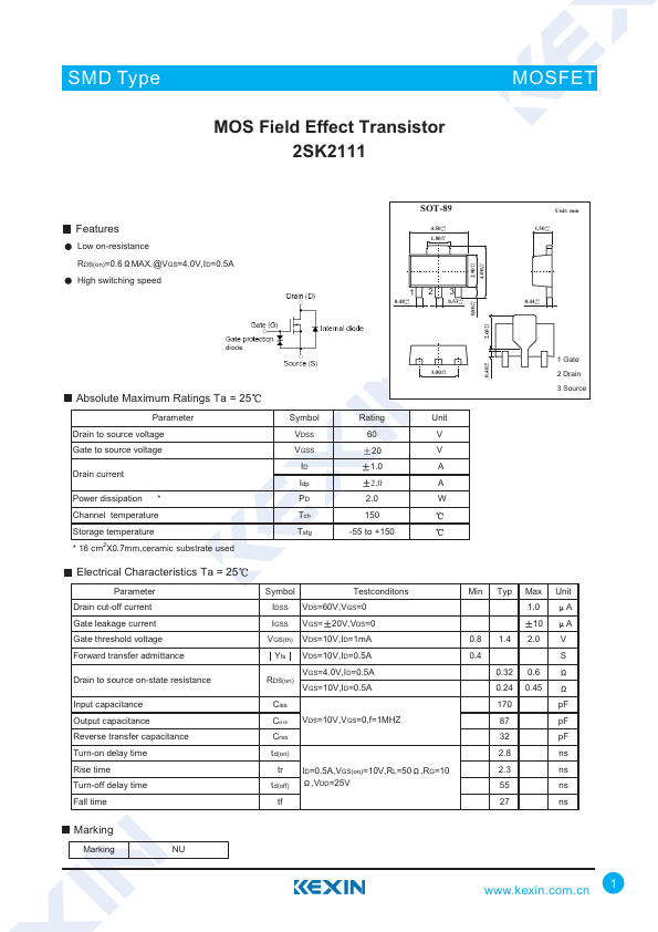
| Description | MOS Field Effect Transistor |
| Datasheet |
 K2111 Datasheet K2111 Datasheet
|
|
|
|
| Part number | K2111 |
|---|---|
| Manufacturer | Kexin |
| File Size | 42.25 KB |
| Description | MOS Field Effect Transistor |
| Datasheet |
K2111 Datasheet
|
|
|
|