Datasheet4U Logo Datasheet4U.com

MPC9120 Datasheet - Motorola

MPC9120 1:10 LVCMOS FANOUT BUFFER

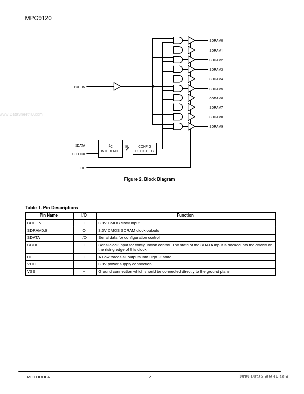
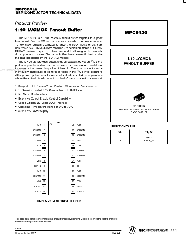
Pin Name BUF_IN SDRAM0:9 SDATA SCLK OE VDD VSS I/O I O I/O I I * * 3.3V CMOS clock input 3.3V CMOS SDRAM clock outputs Serial data for configuration control Serial clock input for configuration control. The state of the SDATA input is clocked into the device on the rising edge of th.

MPC9120 Features

* 10 low skew outputs optimized to drive the clock inputs of standard unbuffered SO

* DIMM SDRAM modules. Standard unbuffered SO

* DIMM SDRAM modules require two clocks per module allowing for the device to drive up to four modules. The output buffers have been optimized to drive the load

MPC9120 Datasheet (98.14 KB)

Preview of MPC9120 PDF
MPC9120 Datasheet Preview Page 2 MPC9120 Datasheet Preview Page 3

Datasheet Details

Part number:

MPC9120

Manufacturer:

Motorola

File Size:

98.14 KB

Description:

1:10 lvcmos fanout buffer.

📁 Related Datasheet

MPC9100 DUAL PLL CLOCK GENERATOR (Motorola)

MPC9108 MULTIPLE OUTPUT CLOCK SYNTHESIZER (Motorola)

MPC9109 LOW VOLTAGE 1:18 CLOCK DISTRIBUTION CHIP (Motorola)

MPC9109 Low Voltage 1:18 Clock Distribution Chip (Integrated Device Technology)

MPC911 LOW-VOLTAGE 1:9 DIFFERENTIAL ECL/HSTL TO HSTL CLOCK DRIVER (Motorola)

MPC9140 1:18 LVCMOS FANOUT BUFFER (Motorola)

MPC9229 400 MHz Low Voltage PECL Clock Synthesizer (Motorola)

MPC9230 800 MHz Low Voltage PECL Clock Synthesizer (Motorola)

TAGS

MPC9120 110 LVCMOS FANOUT BUFFER Motorola

MPC9120 Distributor