Datasheet Details
- Part number
- HD74LVC74
- Manufacturer
- Renesas ↗
- File Size
- 182.10 KB
- Datasheet
- HD74LVC74-Renesas.pdf
- Description
- Dual D-type Flip Flops
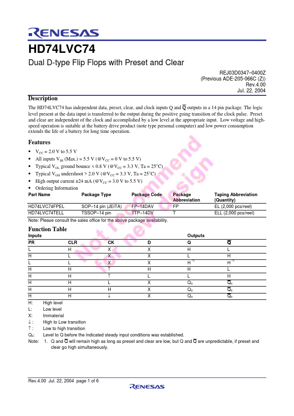
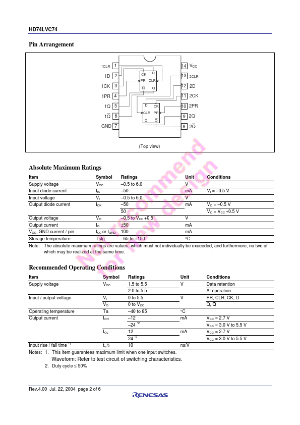
REJ03D0347 0400Z (Previous ADE-205-066C (Z)) Rev.4.00 Jul.22, 2004 The HD74LVC74 has independent data, preset, clear, and clock inputs Q and Q outputs in a 14 pin package.The logic level present at the data input is transferred to the output during the positive going transition of the clock pulse.Preset and clear are independent of the clock and accomplished by a low level at the appropriate input.Low voltage and highspeed operation is suitable at the battery drive product (note ty
📁 Related Datasheet
📌 All Tags
HD74LVC74 Stock/Price