Datasheet Details
| Part number | SLG55321-130010V |
|---|---|
| Manufacturer | Renesas ↗ |
| File Size | 255.03 KB |
| Description | Triple Rail High Voltage Gate Driver |
| Datasheet |
 SLG55321-130010V-Renesas.pdf SLG55321-130010V-Renesas.pdf
|
| Part number | SLG55321-130010V |
|---|---|
| Manufacturer | Renesas ↗ |
| File Size | 255.03 KB |
| Description | Triple Rail High Voltage Gate Driver |
| Datasheet |
SLG55321-130010V-Renesas.pdf
|
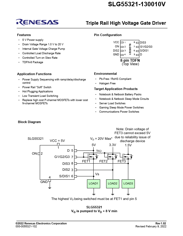
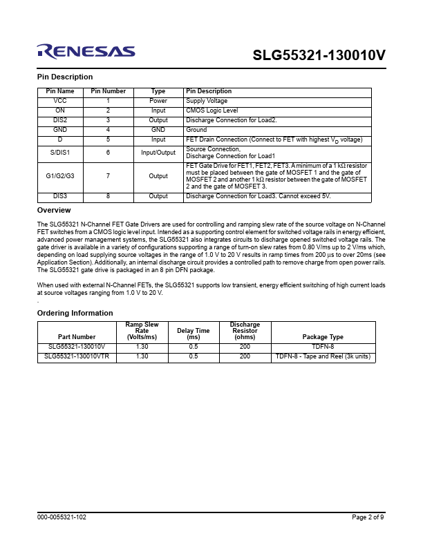
Pin Name VCC ON DIS2 GND D S/DIS1 G1/G2/G3 DIS3 Overview Pin Number 1 2 3 4 5 6 7 8 Type Power Input Output GND Input Input/Output Output Output Pin Description Supply Voltage CMOS Logic Level Discharge Connection for Load2. Ground FET Drain Connection (Connect to FET with highest VD voltage) Source Connection, Discharge Connection for Load1 FET Gate Drive for FET1, FET2, FET3. A minimum of a 1 kΩ resistor must be placed between the gate of MOSFET 1 and the gate of MOSFET 2 and another 1 kΩ
📁 SLG55321-130010V Similar Datasheet