Datasheet Details
- Part number
- CGY181
- Manufacturer
- Siemens Semiconductor Group
- File Size
- 138.00 KB
- Datasheet
- CGY181_SiemensSemiconductorGroup.pdf
- Description
- GaAs MMIC
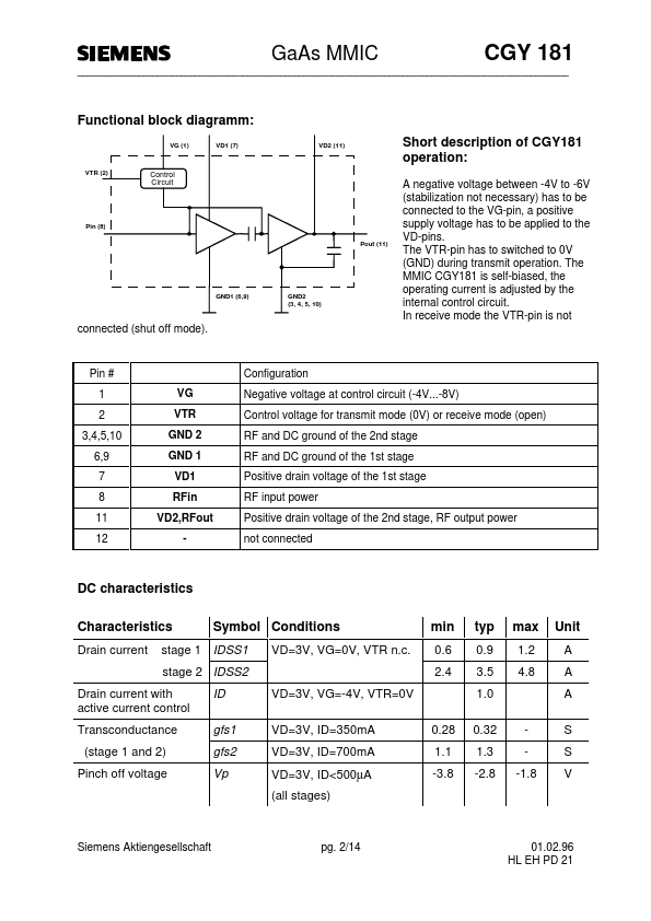
of CGY181 operation: A negative voltage between -4V to -6V (stabilization not necessary) has to be connected to the VG-pin, a positive supply voltage has to be applied to the VD-pins.The VTR-pin has to switched to 0V (GND) during transmit operation.The MMIC CGY181 is self-biased, the operating current is adjusted by the internal control circuit.In receive mode the VTR-pin is not VTR (2) Control Circuit Pin (8) Pout (11) GND1 (6,9) GND2 (3, 4, 5, 10) connected (shut off mode).Pin # 1 2
📁 Related Datasheet
📌 All Tags
CGY181 Stock/Price