The following content is an automatically extracted verbatim text
from the original manufacturer datasheet and is provided for reference purposes only.
View original datasheet text
TOSHIBA Field Effect Transistor Silicon P Channel MOS Type
SSM3J01F
SSM3J01F
High Speed Switching Applications
Unit: mm
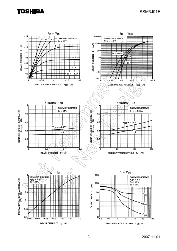
• Small package • Low on resistance : Ron = 0.4 Ω (max) (VGS = −4 V)
: Ron = 0.6 Ω (max) (VGS = −2.5 V) • Low gate threshold voltage
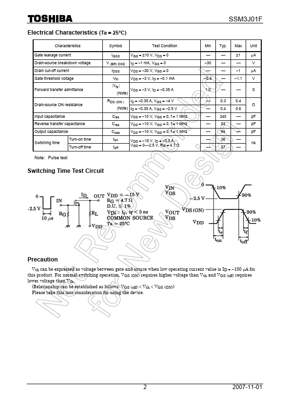
Absolute Maximum Ratings (Ta = 25°C)
Characteristics
Symbol
Rating
Unit
Drain-source voltage
Gate-source voltage
Drain current
DC Pulse
Drain power dissipation (Ta = 25°C)
VDS VGSS
ID IDP PD
−30
V
±10
V
−700 mA
−1400
200
mW
Channel temperature Storage temperature range
Tch
150
°C
Tstg
−55~150
°C
JEDEC
TO-236MOD
Note: Using continuously under heavy loads (e.g. the application of high
JEITA
SC-59
temperature/current/voltage and the significant change in temperature, etc.
 SSM3J01F Datasheet