Datasheet Details
| Part number | AO4401 |
|---|---|
| Manufacturer | Alpha & Omega Semiconductors |
| File Size | 359.14 KB |
| Description | P-Channel MOSFET |
| Datasheet | AO4401_ETC.pdf |
|
|
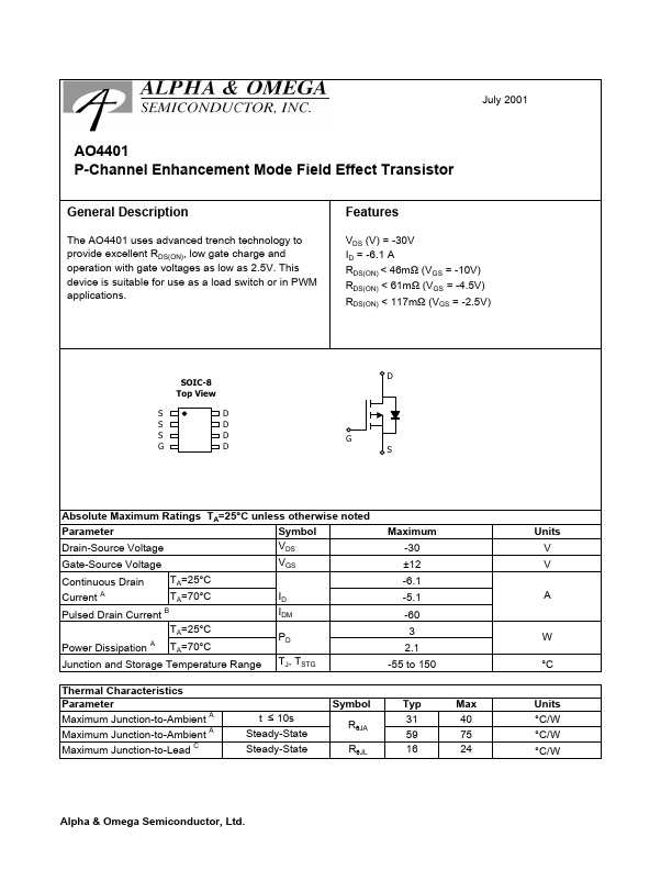
Overview: July 2001 AO4401 P-Channel Enhancement Mode Field Effect Transistor General.
| Part number | AO4401 |
|---|---|
| Manufacturer | Alpha & Omega Semiconductors |
| File Size | 359.14 KB |
| Description | P-Channel MOSFET |
| Datasheet | AO4401_ETC.pdf |
|
|
|
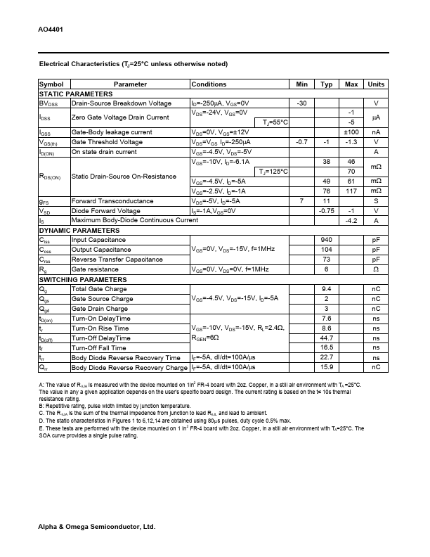
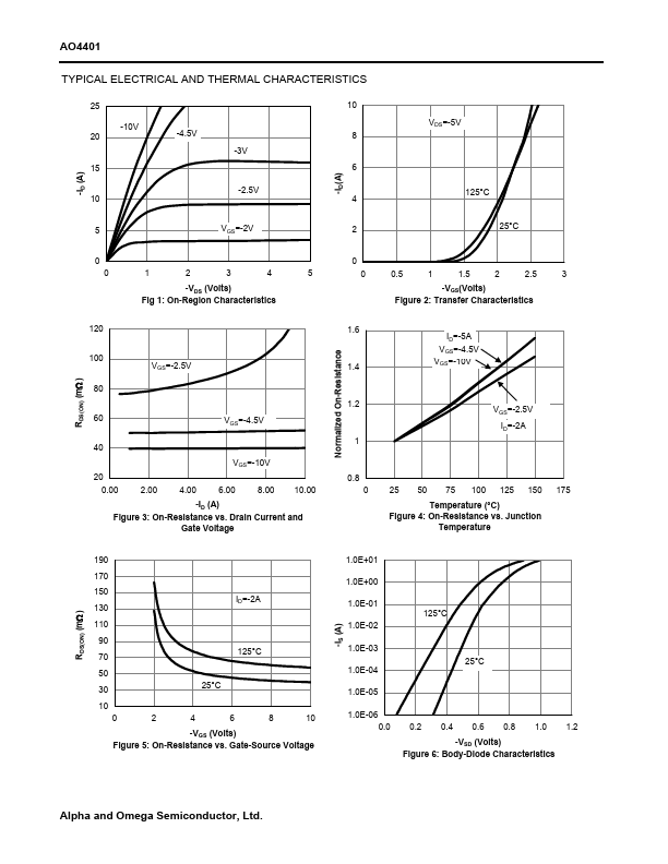
The AO4401 uses advanced trench technology to provide excellent RDS(ON), low gate charge and operation with gate voltages as low as 2.5V.
This device is suitable for use as a load switch or in PWM applications.
| Brand Logo | Part Number | Description | Manufacturer |
|---|---|---|---|
| AO4401 | P-Channel MOSFET | Freescale |
| Part Number | Description |
|---|---|
| AO4400 | N-Channel MOSFET |
| AO4402 | 20V N-Channel MOSFET |
| AO4402G | 20V N-Channel MOSFET |
| AO4403 | 30V P-Channel MOSFET |
| AO4404 | N-Channel MOSFET |
| AO4404B | 30V N-Channel MOSFET |
| AO4405 | 30V P-Channel MOSFET |
| AO4406 | N-Channel MOSFET |
| AO4406A | N-Channel MOSFET |
| AO4406AL | N-Channel MOSFET |