Download the H5N5006LM datasheet PDF.
This datasheet also covers the H5N5006LD variant, as both devices belong to the same (h5n5006xx) silicon n-channel mosfet family and are provided as variant models within a single manufacturer datasheet.
Key Features
Low on-resistance.
Low leakage current.
High speed switching.
Low gate charge.
Avalanche ratings
Outline
LDPAK
G
w
w
w
a . D
D S
S ta
1 2 3
e h
1 2
U 4 t e
4 4
. c
m o
Rev.0 Aug.2002
4
3
1
2
H5N5006LS
3
H5N5006LD
H5N5006LM 1. Gate 2. Drain 3. Source 4. Drain
w
w
w
. D
at
h S a
t e e
4U
. m o c
H5N5006LD, H5N5006LS, H5N5006LM
Absolute Maximum Ratings
(Ta = 25°C)
Item Drain to source voltage Gate to source voltage Drain curr.
Full PDF Text Transcription for H5N5006LM (Reference)
Note: Below is a high-fidelity text extraction (approx. 800 characters) for
H5N5006LM. For precise diagrams, and layout, please refer to the original PDF.
H5N5006LD, H5N5006LS, H5N5006LM Silicon N Channel MOS FET High Speed Power Switching ADE-208-1549 (Z) Features • Low on-resistance • Low leakage current • High speed swit...
View more extracted text
) Features • Low on-resistance • Low leakage current • High speed switching • Low gate charge • Avalanche ratings Outline LDPAK G w w w a .D D S S ta 1 2 3 e h 1 2 U 4 t e 4 4 .c m o Rev.0 Aug.2002 4 3 1 2 H5N5006LS 3 H5N5006LD H5N5006LM 1. Gate 2. Drain 3. Source 4. 
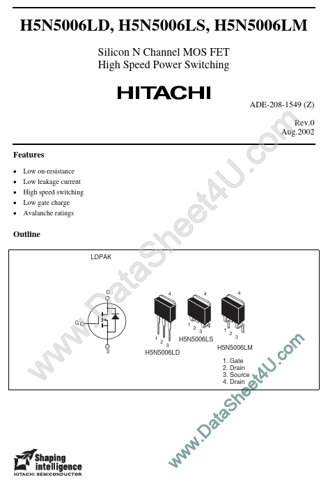
Drain w w w .D at h S a t e e 4U . m o c H5N5006LD, H5N5006LS, H5N5006LM Absolute Maximum Ratings (Ta = 25°C) Item Drain to source voltage Gate to source voltage Drain current Drain peak current Body-drain diode reverse drain current Avalanche current Channel dissipation Channel to case thermal impedance Channel temperature Storage temperature Notes: 1. PW ≤ 1