2SB683 Overview
Description
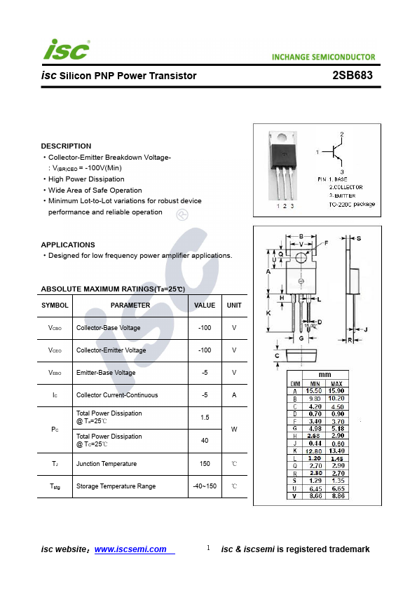
Collector-Emitter Breakdown Voltage- : V(BR)CEO = -100V(Min) - High Power Dissipation - Wide Area of Safe Operation - Minimum Lot-to-Lot variations for robust device performance and reliable operation.
| Part | 2SB683 |
|---|---|
| Description | PNP Transistor |
| Category | Transistor |
| Manufacturer | Inchange Semiconductor |
| Size | 214.56 KB |
Collector-Emitter Breakdown Voltage- : V(BR)CEO = -100V(Min) - High Power Dissipation - Wide Area of Safe Operation - Minimum Lot-to-Lot variations for robust device performance and reliable operation.
| Part Number | Manufacturer | Description |
|---|---|---|
| 2SB688 | Toshiba | Silicon PNP Transistor |
| 2SB688 | Savantic | Silicon PNP Power Transistors |
| B686 | SavantIC | 2SB686 |
| 2SB688 | First Silicon | PNP EPITAXIAL SILICON TRANSISTOR |
| 2SB688 | Unisonic Technologies | SILICON PNP TRANSISTORS |