IRF520VL
Description
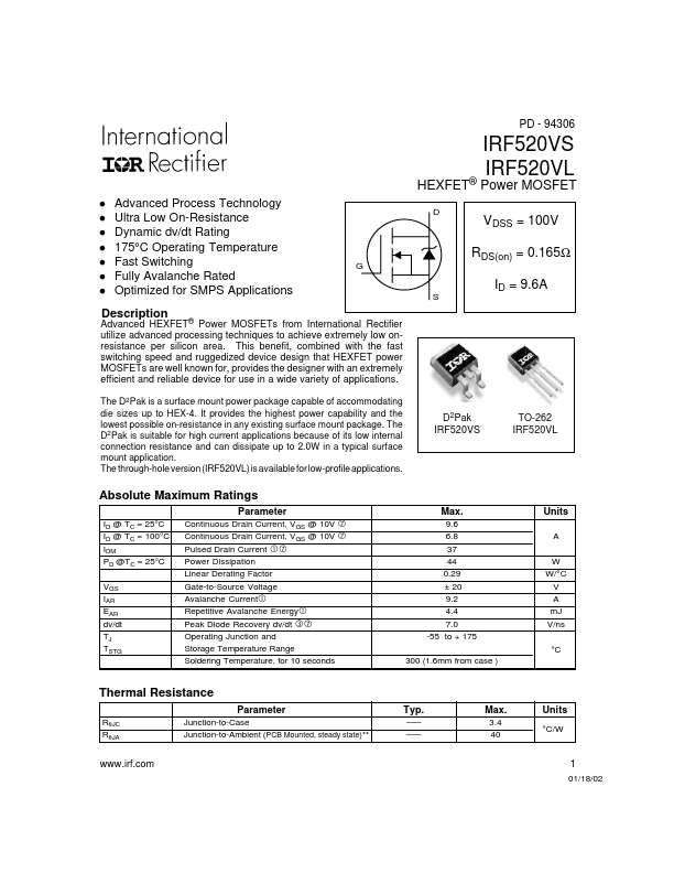
D2Pak IRF520VS
TO-262 IRF520VL
Absolute Maximum Ratings
Parameter
ID @ TC = 25°C ID @ TC = 100°C IDM PD @TC = 25°C VGS IAR EAR dv/dt TJ TSTG Continuous Drain Current, VGS @ 10V Continuous Drain Current, VGS @ 10V Pulsed Drain Current Power Dissipation Linear Derating Factor Gate-to-Source Voltage Avalanche Current Repetitive Avalanche Energy Peak Diode Recovery dv/dt
- Operating Junction and Storage Temperature Range Soldering Temperature, for 10 seconds
Max.
9.6 6.8 37 44 0.29 ± 20 9.2 4.4 7.0 -55 to + 175 300 (1.6mm from case )
Units
A W W/°C V A m J V/ns °C
Thermal Resistance
Parameter
RθJC RθJA Junction-to-Case Junction-to-Ambient ( PCB Mounted, steady state)-
- Typ.
- -
- -
- -
Max.
3.4 40
Units
°C/W
.irf.
01/18/02
IRF520VS/IRF520VL
Electrical Characteristics @ TJ = 25°C (unless otherwise specified)
V(BR)DSS
∆V(BR)DSS/∆TJ
RDS(on) VGS(th) gfs IDSS IGSS Qg Qgs Qgd td(on) tr td(off) tf LD LS Ciss Coss Crss EAS
Parameter Drain-to-Source Breakdown...