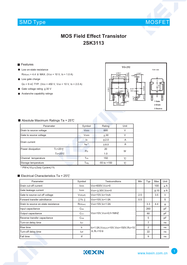
Datasheet4U Logo Datasheet4U.com

2SK3113 - MOS Field Effect Transistor

Key Features

  • Low on-state resistance RDS(on) = 4.4 MAX. (VGS = 10 V, ID = 1.0 A) Low gate charge QG = 9 nC TYP. (VDD = 450 V, VGS = 10 V, ID = 2.0 A) Gate voltage rating 30 V Avalanche capability ratings +0.2 9.70 -0.2 TO-252 6.50+0.15 -0.15 5.30+0.2 -0.2 2.30+0.1 -0.1 0.50+0.8 -0.7 Unit: mm +0.15 1.50 -0.15 3.80 +0.15 5.55 -0.15 0.80+0.1 -0.1 0.127 max 2.3 4.60+0.15 -0.15 0.60+0.1 -0.1 +0.15 0.50 -0.15 +0.28 1.50 -0.1 +0.25 2.65 -0.1 1 Gate 2 Drain 3 Source Absolute Maximum Ratings Ta = 25.

📥 Download Datasheet

Full PDF Text Transcription (Reference)

The following content is an automatically extracted verbatim text from the original manufacturer datasheet and is provided for reference purposes only.

View original datasheet text
SMD Type MOS Field Effect Transistor 2SK3113 MOSFICET Features Low on-state resistance RDS(on) = 4.4 MAX. (VGS = 10 V, ID = 1.0 A) Low gate charge QG = 9 nC TYP. (VDD = 450 V, VGS = 10 V, ID = 2.0 A) Gate voltage rating 30 V Avalanche capability ratings +0.2 9.70 -0.2 TO-252 6.50+0.15 -0.15 5.30+0.2 -0.2 2.30+0.1 -0.1 0.50+0.8 -0.7 Unit: mm +0.15 1.50 -0.15 3.80 +0.15 5.55 -0.15 0.80+0.1 -0.1 0.127 max 2.3 4.60+0.15 -0.15 0.60+0.1 -0.1 +0.15 0.50 -0.15 +0.28 1.50 -0.1 +0.25 2.65 -0.1 1 Gate 2 Drain 3 Source Absolute Maximum Ratings Ta = 25 Parameter Drain to source voltage Gate to source voltage Drain current Power dissipation TC=25 TA=25 Channel temperature Storage temperature * PW 10 s,Duty Cycle 1% Symbol Rating Unit VDSS 600 V VGSS 30 V ID 2.