Datasheet Summary
MOTOROLA
SEMICONDUCTOR TECHNICAL DATA
Dynamic Switch PLL Clock Driver
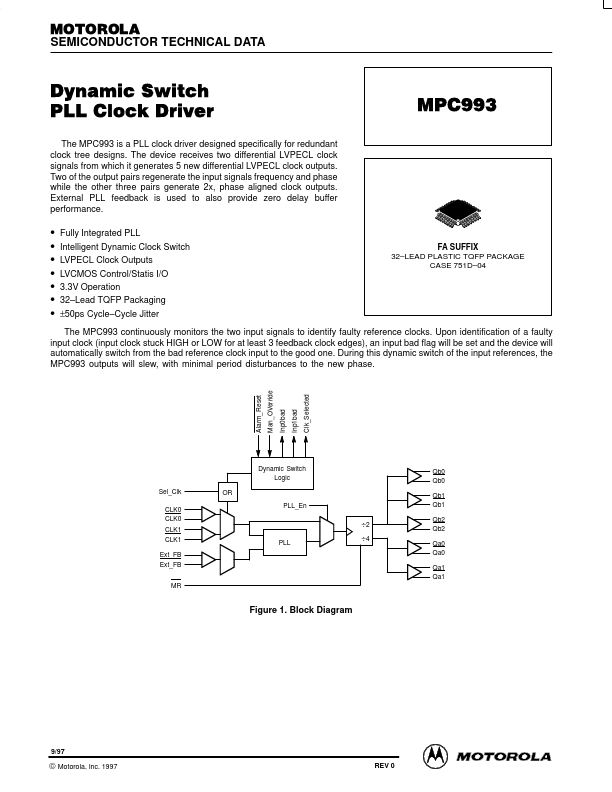
The MPC993 is a PLL clock driver designed specifically for redundant clock tree designs. The device receives two differential LVPECL clock signals from which it generates 5 new differential LVPECL clock outputs. Two of the output pairs regenerate the input signals frequency and phase while the other three pairs generate 2x, phase aligned clock outputs. External PLL feedback is used to also provide zero delay buffer performance.
- -
- -
- -
- Fully Integrated PLL Intelligent Dynamic Clock Switch LVPECL Clock Outputs LVCMOS Control/Statis I/O 3.3V Operation 32- Lead TQFP Packaging ±50ps Cycle- Cycle Jitter
FA...