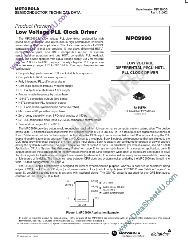
Datasheet4U Logo Datasheet4U.com

MPC9990 - Low Voltage PLL Clock Driver

General Description

Differential clock frequency input Differential feedback input Bank A outputs Bank B outputs Synchronization output Differential feedback output pull-down pull-down pull-down pull-down pull-up pull-up Selection of operating frequency range Selection of bank A output frequency Selection of bank B out

Key Features

  • 500 1000 500 1000 VCC0.6 ±150 400 15 20 mV V µA mA mA Common Mode Ranged CLK, PCLK VCC-1.4 Input high current Power supply current (core) Power supply.

📥 Download Datasheet

Full PDF Text Transcription (Reference)

The following content is an automatically extracted verbatim text from the original manufacturer datasheet and is provided for reference purposes only.

View original datasheet text
MOTOROLA SEMICONDUCTOR TECHNICAL DATA U 4 tPLL Clock Driver Low Voltage e e h S a at .D w w w• 
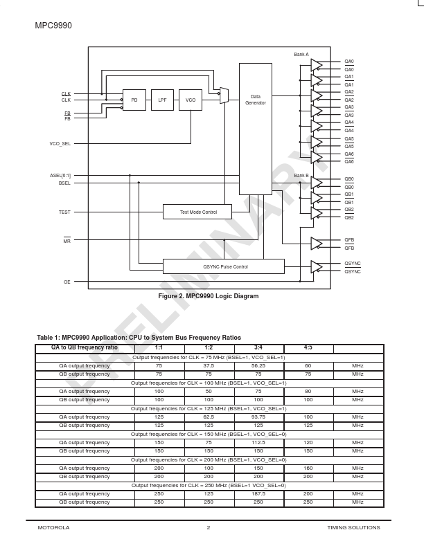
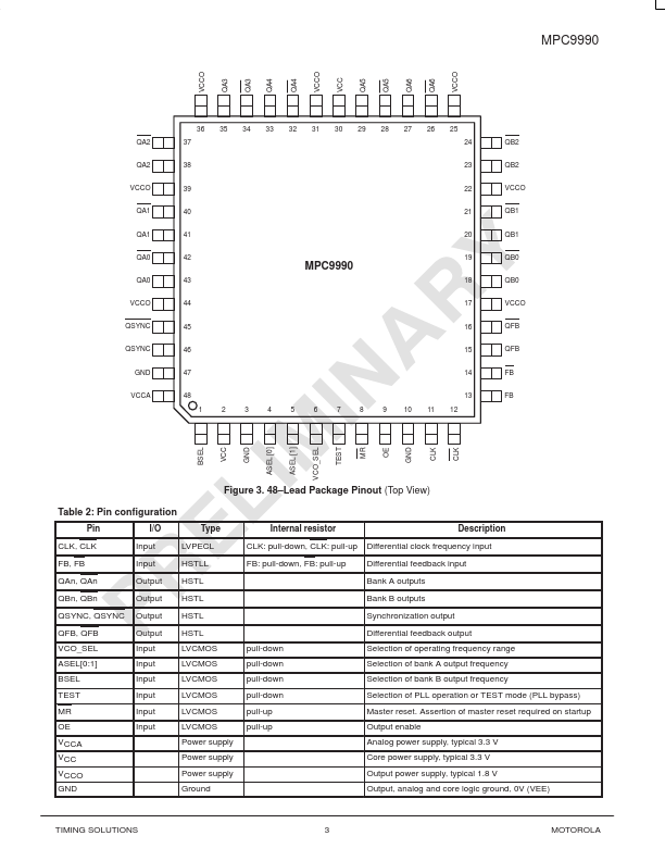
Supports high performance HSTL clock distribution systems Compatible to IA64 processor systems Fully Integrated PLL, differential design Core logic operates from 3.3 V power supply HSTL outputs operate from a 1.8 V supply Programmable frequency by output bank 10 HSTL compatible outputs (two banks) HSTL compatible PLL feedback output HSTL compatible sychronization output (QSYNC) Max. skew of 80 ps within output bank Zero–delay capability: max. SPO (tpd) window of 150 ps Temperature range of 0 to +70°C Product Preview m o .