PK5A7BA
Features
- Pb- Free, Halogen Free and Ro HS pliant.
- Low RDS(on) to Minimize Conduction Losses.
- Ohmic Region Good RDS(on) Ratio.
- Optimized Gate Charge to Minimize Switching Losses.
Applications
- Protection Circuits Applications.
- Logic/Load Switch Circuits Applications.
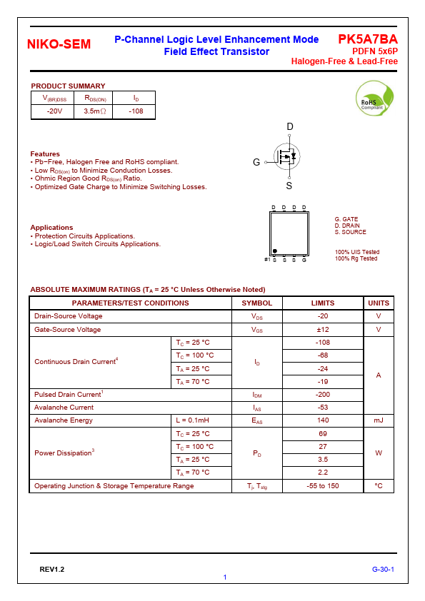
D D DD
#1 S S S G
G. GATE D. DRAIN S. SOURCE
100% UIS Tested 100% Rg Tested
ABSOLUTE MAXIMUM RATINGS (TA = 25 °C Unless Otherwise Noted)
PARAMETERS/TEST CONDITIONS
SYMBOL
Drain-Source Voltage
Gate-Source Voltage
Continuous Drain Current4 Pulsed Drain Current1
TC = 25 °C TC = 100 °C TA = 25 °C TA = 70 °C
Avalanche Current
Avalanche Energy
L = 0.1m H
TC = 25 °C
Power Dissipation3
TC = 100 °C TA = 25 °C
TA = 70 °C
Operating Junction & Storage Temperature Range
VDS VGS
IDM IAS EAS
Tj, Tstg
LIMITS -20 ±12 -108 -68 -24 -19 -200 -53 140 69 27 3.5 2.2
-55 to 150
UNITS V V
A m J W °C
REV1.2
G-30-1...