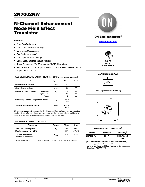
The following content is an automatically extracted verbatim text
from the original manufacturer datasheet and is provided for reference purposes only.
View original datasheet text
2N7002KW
N-Channel Enhancement Mode Field Effect Transistor
Features
• Low On−Resistance • Low Gate Threshold Voltage • Low Input Capacitance • Fast Switching Speed • Low Input/Output Leakage • Ultra−Small Surface Mount Package • These Devices are Pb−Free and are RoHS Compliant • ESD HBM = 1000 V as per JESD22 A114 and ESD CDM = 1500 V
as per JESD22 C101
ABSOLUTE MAXIMUM RATINGS (TA = 25°C unless otherwise noted)
Rating
Symbol Value Unit
Drain−Source Voltage Gate−Source Voltage Maximum Drain Current
Continuous TJ = 100°C
Pulsed
VDSS VGSS
ID
60
V
±20
V
310
mA
195
mA
1.2
A
Operating Junction Temperature Range
TJ
−55 to
°C
+150
Storage Temperature Range
TSTG
−55 to
°C
+150
Stresses exceeding those listed in the Maximum Ratings table may damage the device.