IDT23S05E
IDT23S05E is 3.3V ZERO DELAY CLOCK BUFFER manufactured by Renesas.
IDT23S05E 3.3V ZERO DELAY CLOCK BUFFER, SPREAD SPECTRUM
MERCIAL AND INDUSTRIAL TEMPERATURE RANGES
3.3V ZERO DELAY CLOCK BUFFER, SPREAD SPECTRUM PATIBLE
Features
:
- Phase-Lock Loop Clock Distribution
- 10MHz to 200MHz operating frequency
- Distributes one clock input to one bank of five outputs
- Zero Input-Output Delay
- Output Skew < 250ps
- Low jitter <200 ps cycle-to-cycle
- IDT23S05E-1 for Standard Drive
- IDT23S05E-1H for High Drive
- No external RC network required
- Operates at 3.3V VDD
- Power down mode
- Spread spectrum patible
- Available in SOIC package
DESCRIPTION:
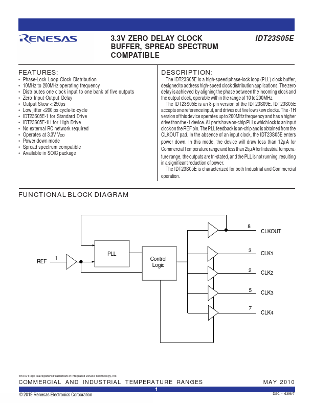
The IDT23S05E is a high-speed phase-lock loop (PLL) clock buffer, designed to address high-speed clock distribution applications. The zero delay is achieved by aligning the phase between the ining clock and the output clock, operable within the range of 10 to 200MHz.
The IDT23S05E is an 8-pin version of the IDT23S09E. IDT23S05E accepts one reference input, and drives out five low skew clocks. The -1H version of this device operates up to 200MHz frequency and has a higher drive than the -1 device. All parts have on-chip PLLs which lock to an input clock on the REF pin. The PLL feedback is on-chip and is obtained from the CLKOUT pad. In the absence of an input clock, the IDT23S05E enters power down. In this mode, the device will draw less than 12µA for mercial Temperature range and less than 25µA for Industrial tempera- ture range, the outputs are tri-stated, and the PLL is not running, resulting in a significant reduction of power.
The IDT23S05E is characterized for both Industrial and mercial operation.
FUNCTIONAL BLOCK DIAGRAM
REF 1
PLL Control
Logic
8 CLKOUT
3 CLK1
2 CLK2
5...