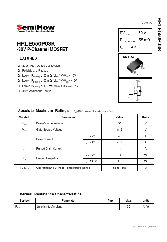
Datasheet4U Logo Datasheet4U.com

HRLE550P03K - P-Channel MOSFET

Key Features

  • ‰ Super High Dense Cell Design ‰ Reliable and Rugged ‰ Lower RDS(ON) : 55 Pȍ (Max. ) @VGS=-10V ‰ Lower RDS(ON) : 65 Pȍ (Max. ) @VGS=-4.5V ‰ Lower RDS(ON) : 100 Pȍ (Max. ) @VGS=-2.5V ‰ 100% Avalanche Tested Feb 2015 BVDSS = - 30 V RDS(on)max = 55 Pȍ ID = - 4 A SOT-23 D S G Absolute Maximum Ratings TA=25୅ unless otherwise specified Symbol Parameter Value VDSS VGS ID IDM PD TJ, TSTG Drain-Source Voltage Gate-Source Voltage Drain Current Pulsed Drain Current TA = 25୅ TA = 70୅ Power Dissipati.

📥 Download Datasheet

Datasheet Details

Part number HRLE550P03K
Manufacturer SemiHow
File Size 667.52 KB
Description P-Channel MOSFET
Datasheet download datasheet HRLE550P03K Datasheet

Full PDF Text Transcription (Reference)

The following content is an automatically extracted verbatim text from the original manufacturer datasheet and is provided for reference purposes only.

View original datasheet text
HRLE550P03K HRLE550P03K -30V P-Channel MOSFET FEATURES ‰ Super High Dense Cell Design ‰ Reliable and Rugged ‰ Lower RDS(ON) : 55 Pȍ (Max.) @VGS=-10V ‰ Lower RDS(ON) : 65 Pȍ (Max.) @VGS=-4.5V ‰ Lower RDS(ON) : 100 Pȍ (Max.) @VGS=-2.5V ‰ 100% Avalanche Tested Feb 2015 BVDSS = - 30 V RDS(on)max = 55 Pȍ ID = - 4 A SOT-23 D S G Absolute Maximum Ratings TA=25୅ unless otherwise specified Symbol Parameter Value VDSS VGS ID IDM PD TJ, TSTG Drain-Source Voltage Gate-Source Voltage Drain Current Pulsed Drain Current TA = 25୅ TA = 70୅ Power Dissipation TA = 25୅ TA = 100୅ Operating and Storage Temperature Range -30 ρ12 -4 -3.1 -12 1.4 0.6 -55 to +150 Units V V A A A W W ୅ Thermal Resistance Characteristics Symbol Parameter RșJA Junction-to-Ambient Typ. -- Max.