P2003ED
P-Channel Enhancement Mode MOSFET
PRODUCT SUMMARY
V(BR)DSS
RDS(ON)
-30V
20mΩ @VGS = -10V
ID -36A
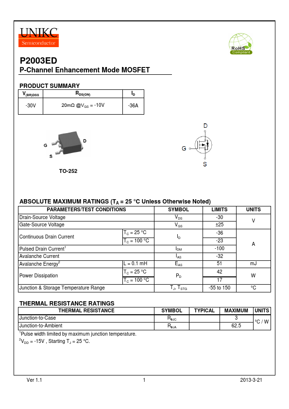
TO-252
ABSOLUTE MAXIMUM RATINGS (TA = 25 °C Unless Otherwise Noted)
PARAMETERS/TEST CONDITIONS
SYMBOL
LIMITS
Drain-Source Voltage
-30
Gate-Source Voltage
±25
Continuous Drain Current Pulsed Drain Current1
TC = 25 °C TC = 100 °C
-36 -23 -100
Avalanche Current Avalanche Energy2
-32
L = 0.1 m H
Power Dissipation
TC = 25 °C
TC = 100 °C
Junction & Storage Temperature Range
TJ, TSTG
-55 to 150
UNITS V
A m J W °C
THERMAL RESISTANCE RATINGS
THERMAL RESISTANCE Junction-to-Case Junction-to-Ambient 1Pulse width limited by maximum junction temperature. 2VDD = -15V , Starting TJ = 25...