BF998 Datasheet
BF998 Datasheet (NXP Semiconductors)
NXP Semiconductors
Depletion type field effect transistor in a plastic microminiature SOT143B or SOT143R package with source and substrate interconnected. The transistors are protected against excessive input voltage su.
* Short channel transistor with high forward transfer
admittance to input capacitance ratio
* Low noise gain controlled amplifier up to 1 GHz.
APPLICATIONS
* VHF and UHF applications with 12 V supply voltage,
such as television tuners and professional communications equipment.
DESCRIPTION
Depletion .
BF998 Datasheet (Vishay)
Vishay
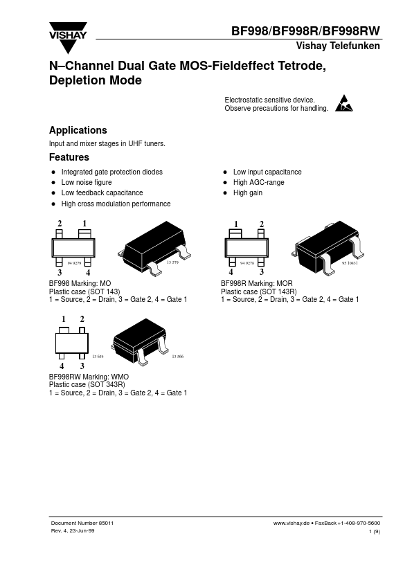
BF998/BF998R/BF998RW Vishay Telefunken N–Channel Dual Gate MOS-Fieldeffect Tetrode, Depletion Mode Electrostatic sensitive device. Observe precautions for handling. Applications Input and mixer stag.
D D D D Integrated gate protection diodes Low noise figure Low feedback capacitance High cross modulation performance D Low input capacitance D High AGC-range D High gain 2 1 1 2 94 9279 13 579 94 9278 95 10831 3 4 4 3 BF998 Marking: MO Plastic case (SOT 143) 1 = Source, 2 = Drain, 3 =.
BF998 Datasheet (Siemens Semiconductor Group)
Siemens Semiconductor Group

Silicon N Channel MOSFET Tetrode BF 998 Features q q Short-channel transistor with high S/C quality factor For low-noise, gain-controlled input stages up to 1 GHz Type BF 998 Marking MO Ordering.
q q Short-channel transistor with high S/C quality factor For low-noise, gain-controlled input stages up to 1 GHz Type BF 998 Marking MO Ordering Code (tape and reel) Q62702-F1129 Pin Configuration 1 2 3 4 S D G2 G1 Package1) SOT-143 Maximum Ratings Parameter Drain-source voltage Drain curren.
BF998 Datasheet (Infineon)
Infineon
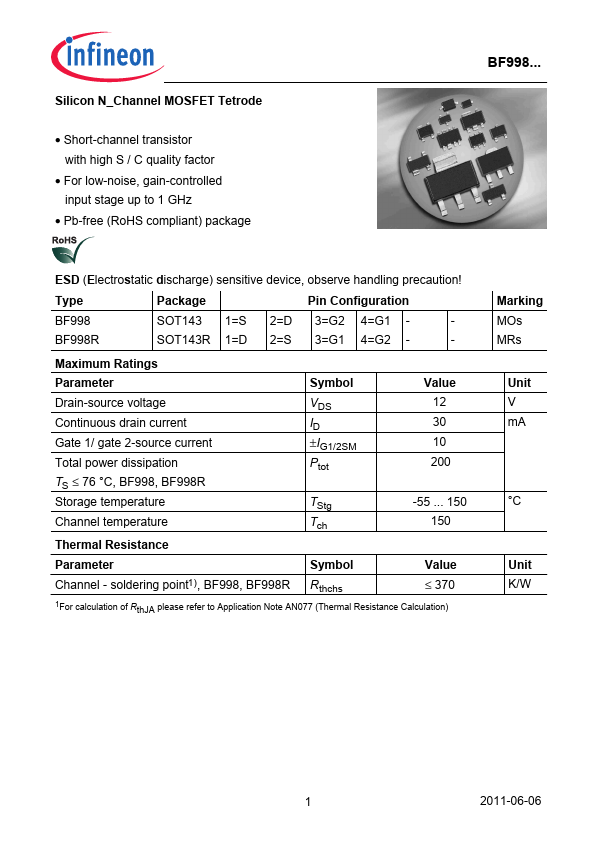
Silicon N_Channel MOSFET Tetrode • Short-channel transistor with high S / C quality factor • For low-noise, gain-controlled input stage up to 1 GHz • Pb-free (RoHS compliant) package BF998... ESD (E.
Symbol Values Unit min. typ. max. DC Characteristics Drain-source breakdown voltage ID = 10 µA, VG1S = -4 V, VG2S = -4 V Gate 1 source breakdown voltage ±IG2S = 10 mA, VG2S = VDS = 0 Gate2 source breakdown voltage ±IG2S = 10 mA, VG2S = VDS = 0 Gate 1 source leakage current ±VG1S = 5 V, VG2S =.