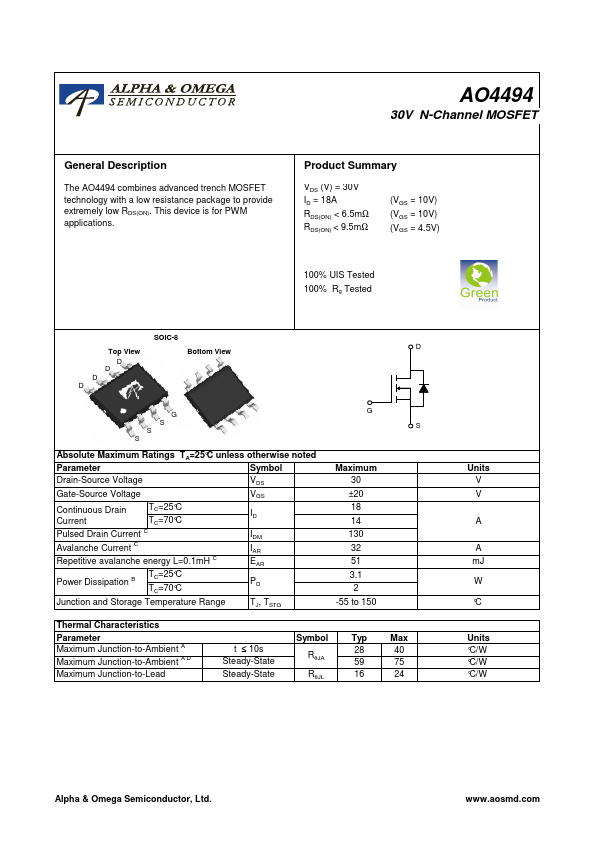
AO4494
Electrical Characteristics (TJ=25°C unless otherwise noted)
Symbol
Parameter
Conditions
Min Typ Max Units
STATIC PARAMETERS
BVDSS Drain-Source Breakdown Voltage
IDSS Zero Gate Voltage Drain Current
ID=250µA, VGS=0V
VDS=30V, VGS=0V
IGSS
VGS(th)
ID(ON)
RDS(ON)
gFS
VSD
IS
Gate-Body leakage current
Gate Threshold Voltage
On state drain current
VDS=0V, VGS= ±20V
VDS=VGS ID=250µA
VGS=10V, VDS=5V
VGS=10V, ID=18A
Static Drain-Source On-Resistance
Forward Transconductance
Diode Forward Voltage
VGS=4.5V, ID=16A
VDS=5V, ID=18A
IS=1A,VGS=0V
Maximum Body-Diode Continuous Current
TJ=125°C
TJ=125°C
30
1.5
130
1
5
±100
2 2.5
5.4
8.4
7.5
70
0.75
6.5
10.1
9.5
1
3
V
µA
nA
V
A
mΩ
mΩ
S
V
A
DYNAMIC PARAMETERS
Ciss Input Capacitance
Coss Output Capacitance
Crss Reverse Transfer Capacitance
Rg Gate resistance
VGS=0V, VDS=15V, f=1MHz
VGS=0V, VDS=0V, f=1MHz
1270
170
87
0.8
1590
240
145
1.5
1900
310
200
2.3
pF
pF
pF
Ω
SWITCHING PARAMETERS
Qg(10V) Total Gate Charge
24 30 36
Qg(4.5V) Total Gate Charge
Qgs Gate Source Charge
VGS=10V, VDS=15V, ID=18A
12 15 18
4.2 5.2 6.2
Qgd Gate Drain Charge
4.7 7.8 11
tD(on)
Turn-On DelayTime
6.7
tr Turn-On Rise Time
VGS=10V, VDS=15V, RL=0.83Ω,
3.5
tD(off)
Turn-Off DelayTime
RGEN=3Ω
22.5
tf Turn-Off Fall Time
4
trr Body Diode Reverse Recovery Time IF=18A, dI/dt=500A/µs
22 28 34
Qrr Body Diode Reverse Recovery Charge IF=18A, dI/dt=500A/µs
19 24 30
nC
nC
nC
nC
ns
ns
ns
ns
ns
nC
A. The value of RθJA is measured with the device mounted on 1in2 FR-4 board with 2oz. Copper, in a still air environment with TA =25°C. The
Power dissipation PDSM is based on R θJA and the maximum allowed junction temperature of 150°C. The value in any given application depends
on the user's specific board design.
B. The power dissipation PD is based on TJ(MAX)=150°C, using junction-to-case thermal resistance, and is more useful in setting the upper
dissipation limit for cases where additional heatsinking is used.
C. Repetitive rating, pulse width limited by junction temperature TJ(MAX)=150°C. Ratings are based on low frequency and duty cycles to keep initial
TJ =25°C.
D. The RθJA is the sum of the thermal impedence from junction to case RθJC and case to ambient.
E. The static characteristics in Figures 1 to 6 are obtained using <300µs pulses, duty cycle 0.5% max.
F. These curves are based on the junction-to-case thermal impedence which is measured with the device mounted to a large heatsink, assuming
a maximum junction temperature of TJ(MAX)=150°C. The SOA curve provides a single pulse ratin g.
Rev1: Nov. 2010
COMPONENTS IN LIFE SUPPORT DEVICES OR SYSTEMS ARE NOT AUTHORIZED. AOS DOES NOT ASSUME ANY LIABILITY ARISING
OUT OF SUCH APPLICATIONS OR USES OF ITS PRODUCTS. AOS RESERVES THE RIGHT TO IMPROVE PRODUCT DESIGN,
FUNCTIONS AND RELIABILITY WITHOUT NOTICE.
Alpha & Omega Semiconductor, Ltd.
www.aosmd.com