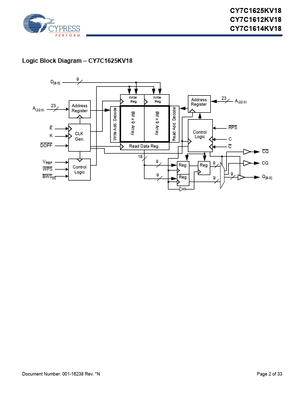
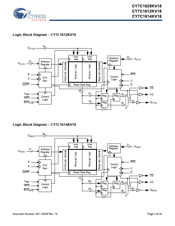
Datasheet4U Logo Datasheet4U.com

CY7C1614KV18 - 144-Mbit QDR II SRAM Two-Word Burst Architecture

Download the CY7C1614KV18 datasheet PDF (CY7C1625KV18 included). The manufacturer datasheet provides complete specifications, pinout details, electrical characteristics, and typical applications for 144-mbit qdr ii sram two-word burst architecture.

Features

  • Separate independent read and write data ports.
  • Supports concurrent transactions.
  • 360-MHz clock for high bandwidth.
  • Two-word burst on all accesses.
  • Double data rate (DDR) interfaces on both read and write ports (data transferred at 720 MHz) at 360 MHz.
  • Two input clocks (K and K) for precise DDR timing.
  • SRAM uses rising edges only.
  • Two input clocks for output data (C and C) to minimize clock skew and flight time mismatches.
  • Echo clocks (CQ and CQ) sim.

📥 Download Datasheet

Note: The manufacturer provides a single datasheet file (CY7C1625KV18-CypressSemiconductor.pdf) that lists specifications for multiple related part numbers.
Other Datasheets by Cypress Semiconductor

Full PDF Text Transcription

Click to expand full text
CY7C1625KV18 CY7C1612KV18 CY7C1614KV18 144-Mbit QDR® II SRAM Two-Word Burst Architecture 144-Mbit QDR® II SRAM Two-Word Burst Architecture Features ■ Separate independent read and write data ports ❐ Supports concurrent transactions ■ 360-MHz clock for high bandwidth ■ Two-word burst on all accesses ■ Double data rate (DDR) interfaces on both read and write ports (data transferred at 720 MHz) at 360 MHz ■ Two input clocks (K and K) for precise DDR timing ❐ SRAM uses rising edges only ■ Two input clocks for output data (C and C) to minimize clock skew and flight time mismatches ■ Echo clocks (CQ and CQ) simplify data capture in high-speed systems ■ Single multiplexed address input bus latches address inputs for both read and write ports ■ Separate port selects for depth expansion ■ Synchron
Published: |