FDMA1025P Overview
Key Specifications
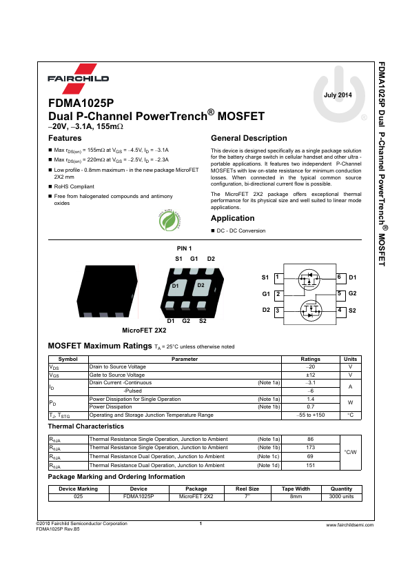
Mount Type: Surface Mount
Pins: 6
Height: 750 µm
Length: 2 mm
Description
July 2014 - Max rDS(on) = 155m: at VGS = –4.5V, ID = –3.1A - Max rDS(on) = 220m: at VGS = –2.5V, ID = –2.3A - Low profile - 0.8mm maximum - in the new package MicroFET 2X2 mm - RoHS Compliant - Free from halogenated compounds and antimony oxides This device is designed specifically as a single package solution for the battery charge switch in cellular handset and other ultra portable applications. It features two independent P-Channel MOSFETs with low on-state resistance for minimum conduction losses.