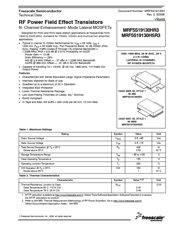
Datasheet4U Logo Datasheet4U.com

MRF5S19130HSR3 - RF Power Field Effect Transistors

Download the MRF5S19130HSR3 datasheet PDF. This datasheet also covers the MRF5S19130HR3 variant, as both devices belong to the same rf power field effect transistors family and are provided as variant models within a single manufacturer datasheet.

Description

Short RF Bead 0.8 pF Chip Capacitor 0.6 4.5 pF Gigatrim Variable Capacitors 2.2 pF Chip Capacitor 1.7 pF Chip Capacitor 9.1 pF Chip Capacitors 1 μF, 25 V Tantalum Capacitors 47 μF, 50 V Electrolytic Capacitor 0.1 μF Chip Capacitors 1000 pF Chip Capacitors 8.2 pF Chip Capacitors 22 μF, 35 V

Features

  • Characterized with Series Equivalent Large - Signal Impedance Parameters.
  • Internally Matched for Ease of Use.
  • Qualified Up to a Maximum of 32 V Operation.
  • Integrated ESD Protection.
  • Lower Thermal Resistance Package.
  • Low Gold Plating Thickness on Leads, 40μ″ Nominal.
  • RoHS Compliant.
  • In Tape and Reel. R3 Suffix = 250 Units per 56 mm, 13 inch Reel. MRF5S19130HR3 MRF5S19130HSR3 1930- 1990 MHz, 26 W AVG. , 28 V 2 x N - CDMA LA.

📥 Download Datasheet

Note: The manufacturer provides a single datasheet file (MRF5S19130HR3_FreescaleSemiconductor.pdf) that lists specifications for multiple related part numbers.

Full PDF Text Transcription

Click to expand full text
www.DataSheet4U.com Freescale Semiconductor Technical Data Document Number: MRF5S19130H Rev. 2, 5/2006 RF Power Field Effect Transistors N - Channel Enhancement - Mode Lateral MOSFETs Designed for PCN and PCS base station applications at frequencies from 1900 to 2000 MHz. Suitable for TDMA, CDMA and multicarrier amplifier applications. • Typical 2 - Carrier N - CDMA Performance for VDD = 28 Volts, IDQ = 1200 mA, Pout = 26 Watts Avg., Full Frequency Band, IS - 95 CDMA (Pilot, Sync, Paging, Traffic Codes 8 Through 13) Channel Bandwidth = 1.2288 MHz. PAR = 9.8 dB @ 0.01% Probability on CCDF. Power Gain — 13 dB Drain Efficiency — 25% IM3 @ 2.5 MHz Offset — - 37 dBc in 1.
Published: |