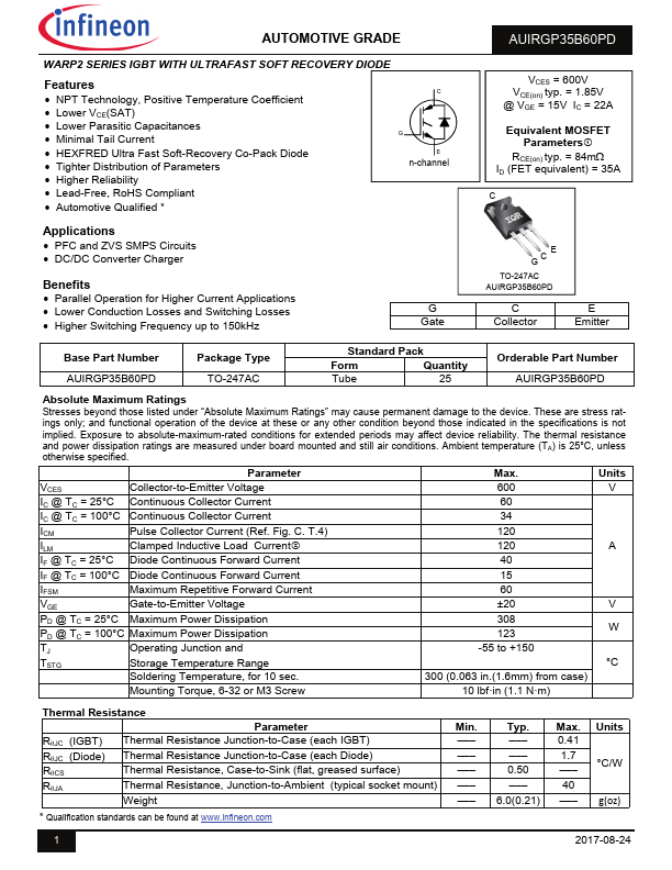
AUIRGP35B60PD
Electrical Characteristics @ TJ = 25°C (unless otherwise specified)
Parameter
Min. Typ.
V(BR)CES
Collector-to-Emitter Breakdown Voltage 600
V(BR)CES/TJ Temperature Coeff. of Breakdown Voltage —
RG
Internal Gate Resistance
—
—
VCE(on)
Collector-to-Emitter Saturation Voltage
—
—
—
0.78
1.7
1.85
2.25
2.37
— 3.00
VGE(th)
VGE(th)/TJ
gfe
ICES
Gate Threshold Voltage
Threshold Voltage temp. coefficient
Forward Transconductance
Collector-to-Emitter Leakage Current
3.0 4.0
— -10
—
36
— 3.0
— 0.35
VFM
Diode Forward Voltage Drop
— 1.30
— 1.20
IGES
Gate-to-Emitter Leakage Current
—
—
Max. Units
Conditions
Ref. Fig.
—
V VGE = 0V, IC = 500µA
— V/°C VGE = 0V, IC = 1mA (25°C-125°C)
— Ω 1MHz, Open Collector
4,5,6,8,9
2.15
IC = 22A, VGE = 15V
2.55
2.80
V
IC = 35A, VGE = 15V
IC = 22A, VGE = 15V, TJ = 125°C
3.45
IC = 35A, VGE = 15V, TJ = 125°C
5.0 V IC = 250µA
— mV/°C VCE = VGE, IC = 1.0mA
—
S VCE = 50V, IC = 22A,PW = 80µs
375 µA VGE = 0V, VCE = 600V
— mA VGE = 0V, VCE = 600V,TJ = 125°C
1.70
1.60
V
IF = 15A
IF = 15A, TJ = 125°C
±100 nA VGE = ±20V, VCE = 0V
7,8,9
10
Switching Characteristics @ TJ = 25°C (unless otherwise specified)
Parameter
Min. Typ. Max. Units
Conditions
Ref. Fig.
Qg
Total Gate Charge (turn-on)
— 160 240
IC = 22A
17
Qge
Gate-to-Emitter Charge (turn-on)
—
55
83 nC VGE = 15V
CT1
Qgc
Gate-to-Collector Charge (turn-on)
— 21 32
VCC = 400V
Eon
Turn-On Switching Loss
— 220 270
Eoff
Turn-Off Switching Loss
— 215 265 J
Etotal
Total Switching Loss
— 435 535
IC = 22A, VCC = 390V,
td(on)
Turn-On delay time
tr
Rise time
— 26 34
VGE = +15V,
— 6.0 8.0 ns RG = 3.3, L = 200µH,
CT3
td(off)
Turn-Off delay time
— 110 122
TJ = 25°C
tf
Eon
Eoff
Etotal
td(on)
tr
td(off)
tf
Cies
Coes
Cres
Fall time
Turn-On Switching Loss
Turn-Off Switching Loss
Total Switching Loss
Turn-On delay time
Rise time
Turn-Off delay time
Fall time
Input Capacitance
Output Capacitance
Reverse Transfer Capacitance
— 8.0 10
— 410 465
— 330 405 J
— 740 870
IC = 22A, VCC = 390V,
— 26 34
VGE = +15V,
— 8.0 11 ns RG = 3.3, L = 200µH,
— 130 150
TJ = 125°C
— 12 16
— 3715 —
— 265 —
— 47 —
VGE = 0V
VCC = 30V
pF f = 1.0Mhz
CT3
11,13
WF1,WF2
CT3
12,14
WF1,WF2
16
Coes eff.
Effective Output Capacitance (Time Related)
— 135 —
Coes eff. (ER) Effective Output Capacitance (Energy Related) —
179
—
RBSOA Reverse Bias Safe Operating Area
FULL SQUARE
VGE = 0V, VCE = 0V to 480V
15
TJ = 150°C, IC = 120A
3
VCC = 480V, Vp ≤ 600V
CT2
trr
Diode Reverse Recovery Time
Qrr
Diode Reverse Recovery Charge
Irr
Peak Reverse Recovery Current
Rg = 22, VGE = +15V to 0V
—
—
—
—
42
74
80
220
60
120
180
600
ns
nC
TJ = 25°C
TJ
TJ
TJ
=
=
=
125°C
25°C
125°C
IF = 15A,
VR = 200V,
di/dt = 200A/µs
19
21
—
—
4.0 6.0
6.5 10
A
TJ = 25°C
TJ = 125°C
19,20,21,22
CT5
Notes:
RCE(on) typ. = equivalent on-resistance = VCE(on) typ./ IC, where VCE(on) typ.= 1.85V and IC =22A. ID (FET Equivalent) is the equivalent MOSFET ID rating @ 25°C for
applications up to 150kHz. These are provided for comparison purposes (only) with equivalent MOSFET solutions.
VCC = 80% (VCES), VGE = 20V, L = 28 µH, RG = 22
Pulse width limited by max. junction temperature.
Energy losses include "tail" and diode reverse recovery, Data generated with use of Diode 30ETH06.
Coes eff. is a fixed capacitance that gives the same charging time as Coes while VCE is rising from 0 to 80% VCES.
Coes eff.(ER) is a fixed capacitance that stores the same energy as Coes while VCE is rising from 0 to 80% VCES.
2
2017-08-24