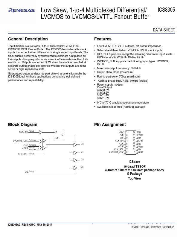
Datasheet4U Logo Datasheet4U.com

ICS8305 - LVCMOS-to-LVCMOS/LVTTL Fanout Buffer

Description

The ICS8305 is a low skew, 1-to-4, Differential/ LVCMOS-toLVCMOS/LVTTL Fanout Buffer.

The ICS8305 has selectable clock inputs that accept either differential or single ended input levels.

Features

  • Four LVCMOS / LVTTL outputs, 7 output impedance.
  • Selectable differential or LVCMOS / LVTTL clock inputs.
  • CLK, nCLK pair can accept the following differential input levels: LVPECL, LVDS, LVHSTL, HCSL, SSTL.
  • LVCMOS_CLK supports the following input types: LVCMOS, LVTTL.
  • Maximum output frequency: 350MHz.
  • Output skew: 35ps (maximum).
  • Part-to-part skew: 700ps (maximum).
  • Additive phase jitter, RMS: 0.04ps (typical).
  • Powe.

📥 Download Datasheet

Datasheet preview – ICS8305

Datasheet Details

Part number ICS8305
Manufacturer Renesas
File Size 832.09 KB
Description LVCMOS-to-LVCMOS/LVTTL Fanout Buffer
Datasheet download datasheet ICS8305 Datasheet
Additional preview pages of the ICS8305 datasheet.
Other Datasheets by Renesas

Full PDF Text Transcription

Click to expand full text
Low Skew, 1-to-4 Multiplexed Differential/ ICS8305 LVCMOS-to-LVCMOS/LVTTL Fanout Buffer DATA SHEET General Description The ICS8305 is a low skew, 1-to-4, Differential/ LVCMOS-toLVCMOS/LVTTL Fanout Buffer. The ICS8305 has selectable clock inputs that accept either differential or single ended input levels. The clock enable is internally synchronized to eliminate runt pulses on the outputs during asynchronous assertion/deassertion of the clock enable pin. Outputs are forced LOW when the clock is disabled. A separate output enable pin controls whether the outputs are in the active or high impedance state. Guaranteed output and part-to-part skew characteristics make the ICS8305 ideal for those applications demanding well defined performance and repeatability.
Published: |