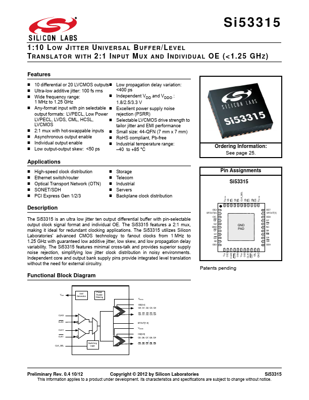
SI53315 Key Features
- 10 differential or 20 LVCMOS outputs- Low propagation delay variation
- Ultra-low additive jitter: 100 fs rms
- Wide frequency range: 1 MHz to 1.25 GHz
- Independent VDD and VDDO : 1.8/2.5/3.3 V
- Any-format input with pin selectable
- Excellent power supply noise
- Selectable LVCMOS drive strength to tailor jitter and EMI performance
- 2:1 mux with hot-swappable inputs
- Small size: 44-QFN (7 mm x 7 mm)
- Asynchronous output enable