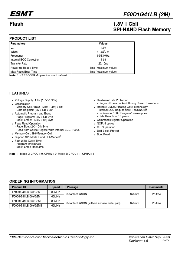

F50D1G41LB-66YG2M Overview
The serial electrical interface follows the industry-standard serial peripheral interface (SPI), providing a cost-effective non-volatile memory storage solution in systems where pin count must be kept to a minimum. The device is a 1Gb SLC SPI-NAND Flash memory device based on the standard parallel NAND Flash, but new mand protocols and registers are defined for SPI operation. It is also an alternative to SPI-NOR,...
F50D1G41LB-66YG2M Key Features
- Voltage Supply: 1.8V (1.7V~1.95V)
- Organization
- Memory Cell Array: (128M + 4M) x 8bit
- Data Register: (2K + 64) x 8bit
- Automatic Program and Erase
- Page Program: (2K + 64) Byte
- Block Erase: (128K + 4K) Byte
- Page Read Operation
- Page Size: (2K + 64) Byte
- Read from Cell to Register with Internal ECC: 100us