Datasheet4U Logo Datasheet4U.com

HD74LVC74

Dual D-type Flip Flops with Preset and Clear

HD74LVC74 Features

* VCC = 2.0 V to 5.5 V All inputs VIH (Max.) = 5.5 V (@VCC = 0 V to 5.5 V) Typical VOL ground bounce < 0.8 V (@VCC = 3.3 V, Ta = 25°C) Typical VOH undershoot > 2.0 V (@VCC = 3.3 V, Ta = 25°C) High output current ±24 mA (@VCC = 3.0 V to 5.5 V) HD74LVC7

HD74LVC74 General Description

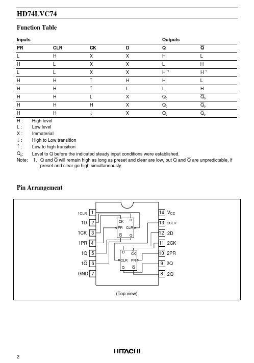
The HD74LVC74 has independent data, preset, clear, and clock inputs Q and Q outputs in a 14 pin package. The logic level present at the data input is transferred to the output during the positive going transition of the clock pulse. Preset and clear are independent of the clock and accomplished by a.

HD74LVC74 Datasheet (48.33 KB)

Preview of HD74LVC74 PDF

Datasheet Details

Part number:

HD74LVC74

Manufacturer:

Hitachi Semiconductor

File Size:

48.33 KB

Description:

Dual d-type flip flops with preset and clear.

📁 Related Datasheet

HD74LVC74 Dual D-type Flip Flops (Renesas)

HD74LVC00 Quad. 2-input NAND Gates (Hitachi Semiconductor)

HD74LVC00 Quad. 2-input NAND Gates (Renesas)

HD74LVC02 Quad. 2-input NOR Gates (Hitachi Semiconductor)

HD74LVC02 Quad. 2-input NOR Gates (Renesas)

HD74LVC04 Hex Inverters (Hitachi Semiconductor)

HD74LVC04 Hex Inverters (Renesas)

HD74LVC08 Quad. 2-input AND Gates (Hitachi Semiconductor)

HD74LVC08 Quad. 2-input AND Gates (Renesas)

HD74LVC125A Quad. Bus Buffer Gates with 3-state Outputs (Hitachi Semiconductor)

TAGS

HD74LVC74 Dual D-type Flip Flops with Preset and Clear Hitachi Semiconductor

Image Gallery

HD74LVC74 Datasheet Preview Page 2 HD74LVC74 Datasheet Preview Page 3

HD74LVC74 Distributor