Datasheet4U Logo Datasheet4U.com

MT47H128M8 - DDR2 SDRAM

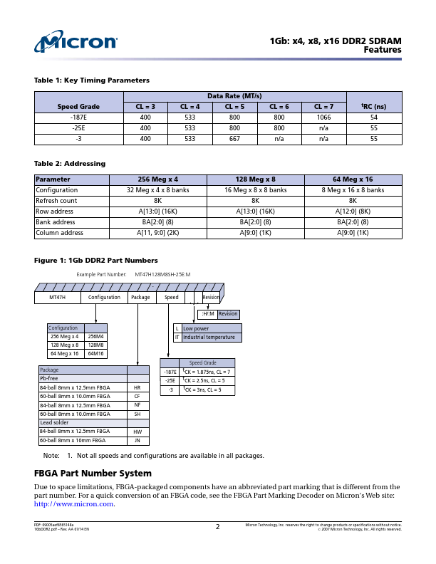
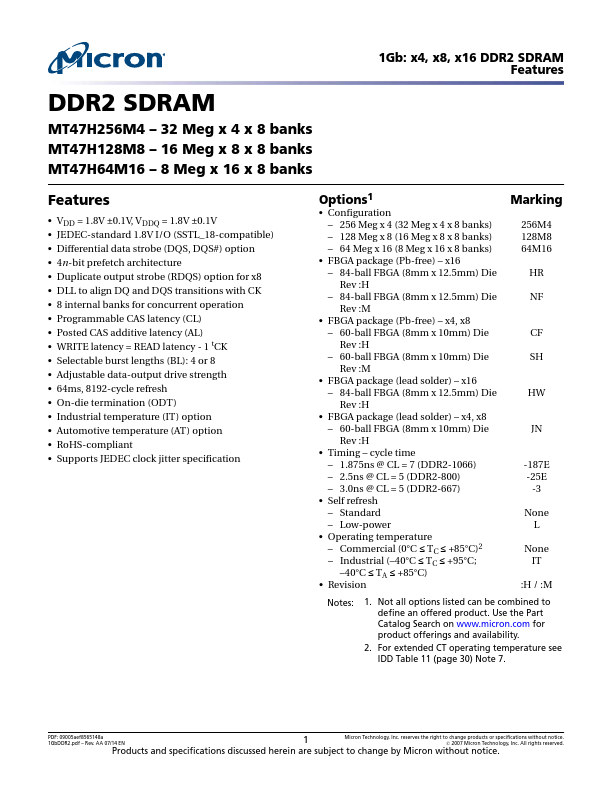
This page provides the datasheet information for the MT47H128M8, a member of the MT47H256M4 DDR2 SDRAM family.

Features

  • Features.
  • VDD = 1.8V ±0.1V, VDDQ = 1.8V ±0.1V.
  • JEDEC-standard 1.8V I/O (SSTL_18-compatible).
  • Differential data strobe (DQS, DQS#) option.
  • 4n-bit prefetch architecture.
  • Duplicate output strobe (RDQS) option for x8.
  • DLL to align DQ and DQS transitions with CK.
  • 8 internal banks for concurrent operation.
  • Programmable CAS latency (CL).
  • Posted CAS additive latency (AL).
  • WRITE latency = READ latency - 1 tCK.

📥 Download Datasheet

Datasheet preview – MT47H128M8

Datasheet Details

Part number MT47H128M8
Manufacturer Micron Technology
File Size 9.35 MB
Description DDR2 SDRAM
Datasheet download datasheet MT47H128M8 Datasheet
Additional preview pages of the MT47H128M8 datasheet.
Other Datasheets by Micron Technology

Full PDF Text Transcription

Click to expand full text
DDR2 SDRAM MT47H256M4 – 32 Meg x 4 x 8 banks MT47H128M8 – 16 Meg x 8 x 8 banks MT47H64M16 – 8 Meg x 16 x 8 banks 1Gb: x4, x8, x16 DDR2 SDRAM Features Features • VDD = 1.8V ±0.1V, VDDQ = 1.8V ±0.1V • JEDEC-standard 1.
Published: |