2SJ494
2SJ494 is P-Channel MOSFET manufactured by NEC.
DESCRIPTION
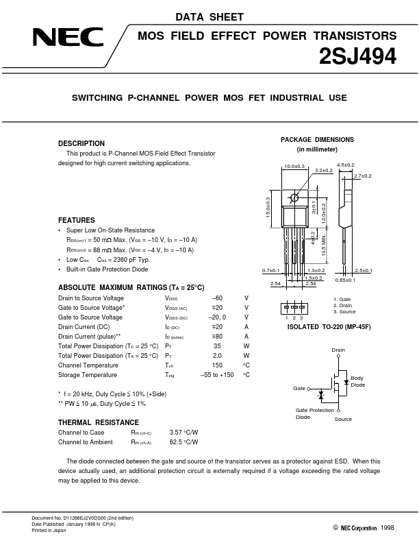
This product is P-Channel MOS Field Effect Transistor designed for high current switching applications.
PACKAGE DIMENSIONS (in millimeter)
10.0±0.3 4.5±0.2 3.2±0.2 2.7±0.2
15.0±0.3
3±0.1 4±0.2
FEATURES
- Super Low On-State Resistance RDS(on)1 = 50 m: Max. (VGS =
- 10 V, ID =
- 10 A) RDS(on)2 = 88 m: Max. (VGS =
- 4 V, ID =
- 10 A)
- Low Ciss Ciss = 2360 p F Typ.
0.7±0.1 2.54
- Built-in Gate Protection Diode
13.5 MIN.
12.0±0.2
ABSOLUTE MAXIMUM RATINGS (TA = 25°C)
Drain to Source Voltage Gate to Source Voltage- Gate to Source Voltage Drain Current (DC) Drain Current (pulse)-
- Total Power Dissipation (TC = 25 °C) Total Power Dissipation (TA = 25 °C) Channel Temperature Storage Temperature VDSS VGSS (AC) VGSS (DC) ID (DC) ID (pulse) PT PT Tch Tstg
- 60
- +20
- 20, 0
- +20
- +80 35 2.0 150
- 55 to +150 V V V A A W W °C °C
1.3±0.2 1.5±0.2 2.54
2.5±0.1 0.65±0.1
1. Gate 2. Drain 3. Source 1 2 3
ISOLATED TO-220 (MP-45F)
Drain
- f = 20 k Hz, Duty Cycle d 10% (+Side)
- - PW d 10 Ps, Duty Cycle d 1%
Gate
Body Diode
THERMAL RESISTANCE
Channel to Case Channel to Ambient Rth (ch-C) Rth (ch-A) 3.57 °C/W 62.5 °C/W
Gate Protection Diode Source
The diode connected between the gate and source of the transistor serves as a protector against ESD. When this device actually used, an additional protection circuit is externally required if a voltage exceeding the rated voltage may be applied to this device.
Document No. D11266EJ2V0DS00 (2nd edition) Date Published January 1998 N CP(K) Printed in...