Datasheet Details
| Part number | 74AUP2G07 |
|---|---|
| Manufacturer | NXP Semiconductors |
| File Size | 124.67 KB |
| Description | Low-power dual buffer |
| Datasheet |
 74AUP2G07 Datasheet 74AUP2G07 Datasheet
|
|
|
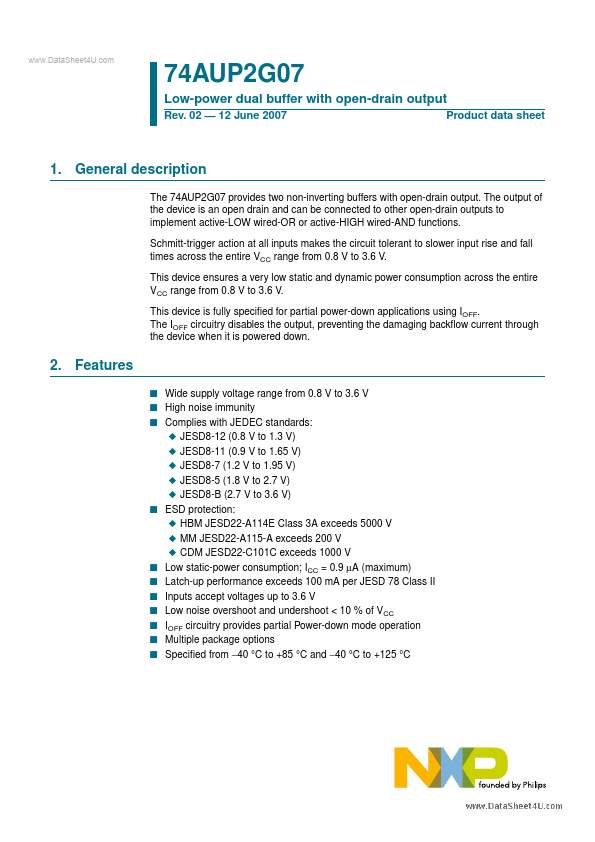
The 74AUP2G07 provides two non-inverting buffers with open-drain output.
The output of the device is an open drain and can be connected to other open-drain outputs to implement active-LOW wired-OR or active-HIGH wired-AND functions.
| Part number | 74AUP2G07 |
|---|---|
| Manufacturer | NXP Semiconductors |
| File Size | 124.67 KB |
| Description | Low-power dual buffer |
| Datasheet |
74AUP2G07 Datasheet
|
|
|
|