Datasheet4U Logo Datasheet4U.com

PLL102-04

Low Skew Output Buffer

PLL102-04 Features

* Frequency range 50 ~ 120MHz. Internal phase locked loop will allow spread spectrum modulation on reference clock to pass to the outputs (up to 100kHz SST modulation).

* Zero input - output delay.

* Less than 700 ps device - device skew.

* Less than 250 ps skew between outputs

PLL102-04 General Description

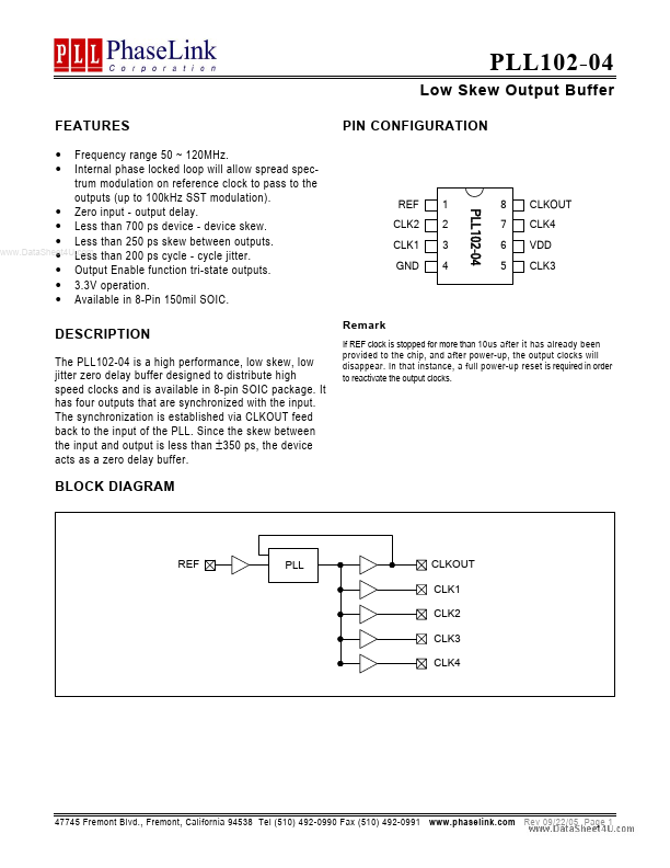
The PLL102-04 is a high performance, low skew, low jitter zero delay buffer designed to distribute high speed clocks and is available in 8-pin SOIC package. It has four outputs that are synchronized with the input. The synchronization is established via CLKOUT feed back to the input of the PLL. Sinc.

PLL102-04 Datasheet (269.36 KB)

Preview of PLL102-04 PDF

Datasheet Details

Part number:

PLL102-04

Manufacturer:

PhaseLink Corporation

File Size:

269.36 KB

Description:

Low skew output buffer.

📁 Related Datasheet

PLL102-03 Low Skew Output Buffer (PhaseLink Corporation)

PLL102-05 Low Skew Output Buffer (PhaseLink Corporation)

PLL102-10 Low Skew Output Buffer (PhaseLink Corporation)

PLL102-108 Programmable DDR Zero Delay Clock Driver (PhaseLink Corporation)

PLL102-109 Programmable DDR Zero Delay Clock Driver (PhaseLink Corporation)

PLL102-15 Low Skew Output Buffer (PhaseLink Corporation)

PLL1000A PHASE LOCKED LOOP (Z-Communications)

PLL103-01 Low Skew Buffer (PhaseLink Corporation)

PLL103-02 DDR SDRAM Buffer (PhaseLink Corporation)

PLL103-03 DDR SDRAM Buffer (PhaseLink Corporation)

TAGS

PLL102-04 Low Skew Output Buffer PhaseLink Corporation

Image Gallery

PLL102-04 Datasheet Preview Page 2 PLL102-04 Datasheet Preview Page 3

PLL102-04 Distributor