Datasheet4U Logo Datasheet4U.com

PLL102-109

Programmable DDR Zero Delay Clock Driver

PLL102-109 Features

* PLL clock distribution optimized for Double Data Rate SDRAM application up to 266Mhz.

* Distributes one clock Input to one bank of six differential outputs.

* Track spread spectrum clocking for EMI reduction.

* Programmable delay between CLK_INT and CLK[T/C] from

* 0.8

PLL102-109 General Description

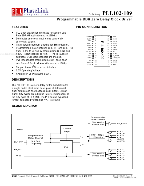
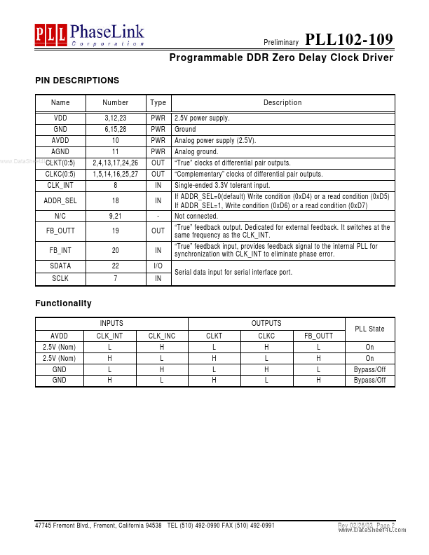
The PLL102-109 is a zero delay buffer that distributes a single-ended clock input to six pairs of differential clock outputs and one feedback clock output. Output signal duty cycles are adjusted to 50%, independent of the duty cycle at CLK_INT. The PLL can be bypassed for test purposes by strapping.

PLL102-109 Datasheet (199.76 KB)

Preview of PLL102-109 PDF

Datasheet Details

Part number:

PLL102-109

Manufacturer:

PhaseLink Corporation

File Size:

199.76 KB

Description:

Programmable ddr zero delay clock driver.

📁 Related Datasheet

PLL102-10 Low Skew Output Buffer (PhaseLink Corporation)

PLL102-108 Programmable DDR Zero Delay Clock Driver (PhaseLink Corporation)

PLL102-15 Low Skew Output Buffer (PhaseLink Corporation)

PLL102-03 Low Skew Output Buffer (PhaseLink Corporation)

PLL102-04 Low Skew Output Buffer (PhaseLink Corporation)

PLL102-05 Low Skew Output Buffer (PhaseLink Corporation)

PLL1000A PHASE LOCKED LOOP (Z-Communications)

PLL103-01 Low Skew Buffer (PhaseLink Corporation)

PLL103-02 DDR SDRAM Buffer (PhaseLink Corporation)

PLL103-03 DDR SDRAM Buffer (PhaseLink Corporation)

TAGS

PLL102-109 Programmable DDR Zero Delay Clock Driver PhaseLink Corporation

Image Gallery

PLL102-109 Datasheet Preview Page 2 PLL102-109 Datasheet Preview Page 3

PLL102-109 Distributor