Datasheet Details
| Part number | LC895925 |
|---|---|
| Manufacturer | Sanyo |
| File Size | 90.01 KB |
| Description | Signal Processing LSI |
| Datasheet |
 LC895925_SanyoSemiconDevice.pdf LC895925_SanyoSemiconDevice.pdf
|
| Part number | LC895925 |
|---|---|
| Manufacturer | Sanyo |
| File Size | 90.01 KB |
| Description | Signal Processing LSI |
| Datasheet |
LC895925_SanyoSemiconDevice.pdf
|
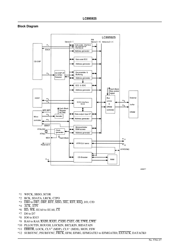
Type: I: Input pin, O: Output pin, B: Bidirectional pin, P: Power supply pin, N: No connection pin Pin Number 1 2 3 4 5 6 7 8 9 10 11 12 13 14 15 16 17 18 19 20 21 22 23 24 25 26 27 28 29 30 31 32 33 34 35 36 37 38 39 40 41 Pin Name VSS Reserve0 Reserve1 Reserve2 TEST1 XTALCK0 XTAL0 TEST2 MCK TEST3 XTALCK1 XTAL1 TEST4 VDD VSS CLV+ (MDP) CLV (MDS) MON FSW VDD VSS PLLOUTIN ROUGH LOCKIN LOCK ERROR ATIPSYNC BIDATAI BICLKIN VDD IO0 IO1 IO2 IO3 IO4 IO5 IO6 IO7 IO8 VDD VSS Type P B B B I I O
📁 LC895925 Similar Datasheet