Datasheet Details
| Part number | CDCLVD110A |
|---|---|
| Manufacturer | Texas Instruments ↗ |
| File Size | 2.06 MB |
| Description | PROGRAMMABLE LOW-VOLTAGE 1:10 LVDS CLOCK DRIVER |
| Datasheet |
 CDCLVD110A-etcTI.pdf CDCLVD110A-etcTI.pdf
|
| Part number | CDCLVD110A |
|---|---|
| Manufacturer | Texas Instruments ↗ |
| File Size | 2.06 MB |
| Description | PROGRAMMABLE LOW-VOLTAGE 1:10 LVDS CLOCK DRIVER |
| Datasheet |
CDCLVD110A-etcTI.pdf
|
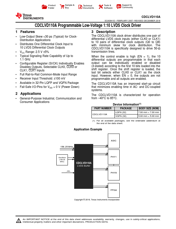
The CDCLVD110A clock driver distributes one pair of differential LVDS clock inputs (either CLK0 or CLK1) to 10 pairs of differential clock outputs (Q0 to Q9) with minimum skew for clock distribution.
📁 CDCLVD110A Similar Datasheet