Datasheet Details
| Part number | CDCLVD1213 |
|---|---|
| Manufacturer | Texas Instruments ↗ |
| File Size | 874.40 KB |
| Description | 1:4 Low Additive Jitter LVDS Buffer |
| Datasheet |
 CDCLVD1213-etcTI.pdf CDCLVD1213-etcTI.pdf
|
| Part number | CDCLVD1213 |
|---|---|
| Manufacturer | Texas Instruments ↗ |
| File Size | 874.40 KB |
| Description | 1:4 Low Additive Jitter LVDS Buffer |
| Datasheet |
CDCLVD1213-etcTI.pdf
|
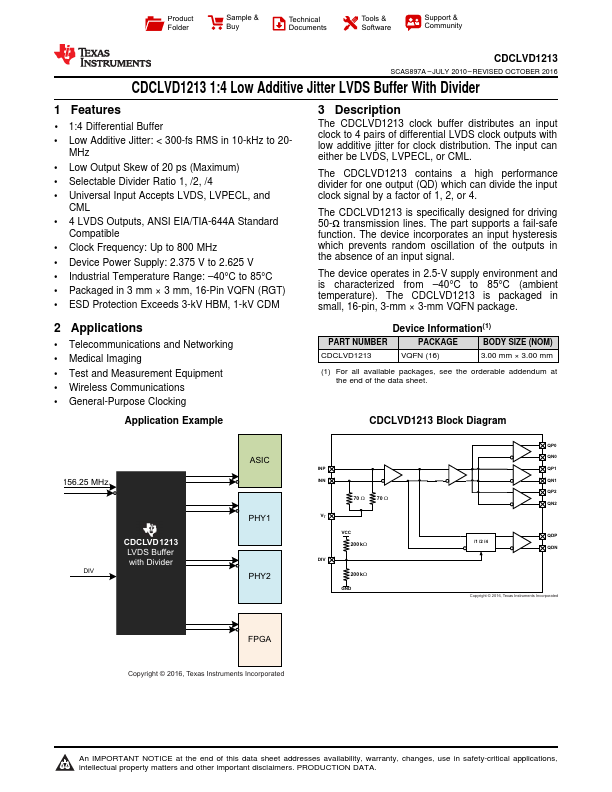
The CDCLVD1213 clock buffer distributes an input clock to 4 pairs of differential LVDS clock outputs with low additive jitter for clock distribution.
📁 CDCLVD1213 Similar Datasheet