Datasheet Details
| Part number | CDCLVD1212 |
|---|---|
| Manufacturer | Texas Instruments ↗ |
| File Size | 1.10 MB |
| Description | 2:12 Low Additive Jitter LVDS Buffer |
| Datasheet |
 CDCLVD1212-etcTI.pdf CDCLVD1212-etcTI.pdf
|
| Part number | CDCLVD1212 |
|---|---|
| Manufacturer | Texas Instruments ↗ |
| File Size | 1.10 MB |
| Description | 2:12 Low Additive Jitter LVDS Buffer |
| Datasheet |
CDCLVD1212-etcTI.pdf
|
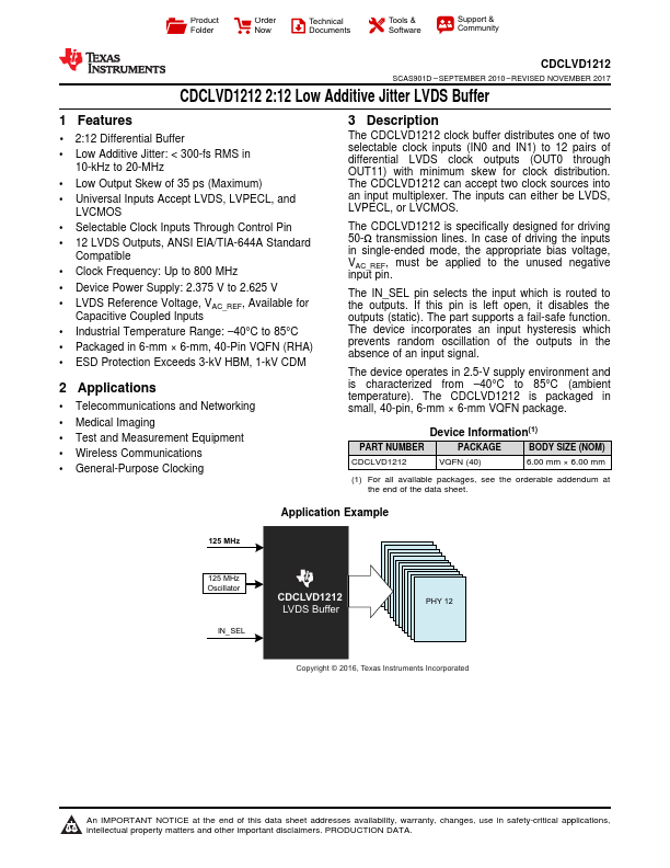
The CDCLVD1212 clock buffer distributes one of two selectable clock inputs (IN0 and IN1) to 12 pairs of differential LVDS clock outputs (OUT0 through OUT11) with minimum skew for clock distribution.
📁 CDCLVD1212 Similar Datasheet