Datasheet Details
| Part number | CDCLVD1208 |
|---|---|
| Manufacturer | Texas Instruments ↗ |
| File Size | 873.51 KB |
| Description | 2:8 Low Additive Jitter LVDS Buffer |
| Datasheet |
 CDCLVD1208-etcTI.pdf CDCLVD1208-etcTI.pdf
|
| Part number | CDCLVD1208 |
|---|---|
| Manufacturer | Texas Instruments ↗ |
| File Size | 873.51 KB |
| Description | 2:8 Low Additive Jitter LVDS Buffer |
| Datasheet |
CDCLVD1208-etcTI.pdf
|
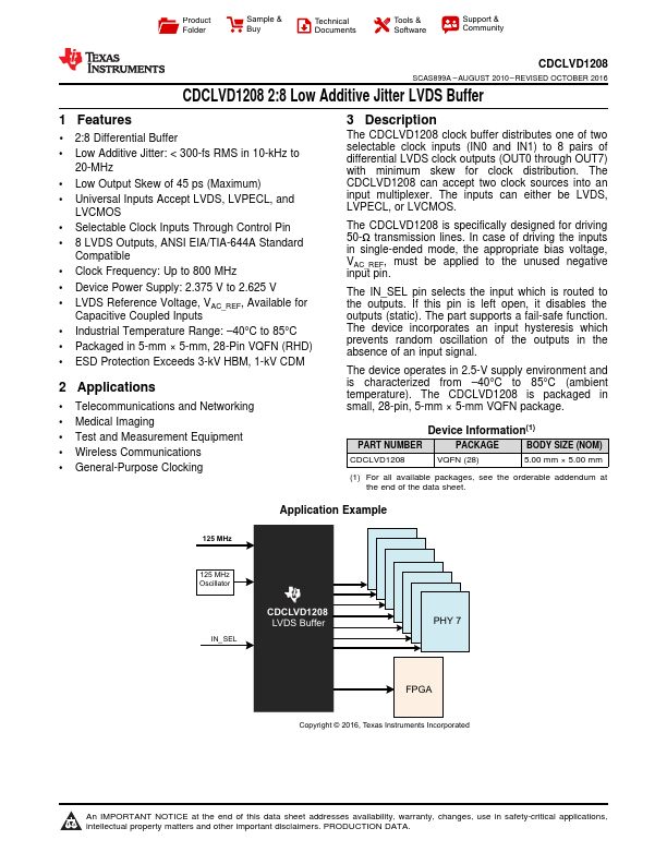
The CDCLVD1208 clock buffer distributes one of two selectable clock inputs (IN0 and IN1) to 8 pairs of differential LVDS clock outputs (OUT0 through OUT7) with minimum skew for clock distribution.
📁 CDCLVD1208 Similar Datasheet