Datasheet Details
| Part number | AO6603 |
|---|---|
| Manufacturer | Alpha & Omega Semiconductors |
| File Size | 315.24 KB |
| Description | MOSFET |
| Datasheet |
 AO6603 Datasheet AO6603 Datasheet
|
|
|
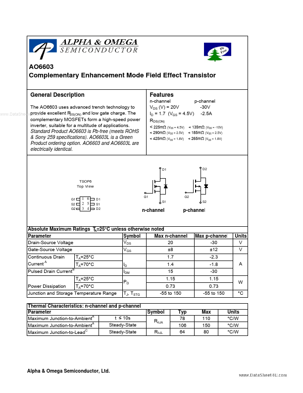
The AO6603 uses advanced trench technology to provide excellent R www.DataSheet4U.com DS(ON) and low gate charge.
The complementary MOSFETs form a high-speed power inverter, suitable for a multitude of applications.
Standard Product AO6603 is Pb-free (meets ROHS & Sony 259 specifications).
| Part number | AO6603 |
|---|---|
| Manufacturer | Alpha & Omega Semiconductors |
| File Size | 315.24 KB |
| Description | MOSFET |
| Datasheet |
AO6603 Datasheet
|
|
|
|
| Part Number | Description | Manufacturer |
|---|---|---|
| AO6601 | N- and P-Channel 20V MOSFET | VBsemi |
| AO6604 | Dual-Channel MOSFET | VBsemi |
| AO6400 | N-Channel MOSFET | Kexin |
| AO6401 | P-Channel MOSFET | Kexin |
| AO6401A | P-Channel MOSFET | Kexin |
| Part Number | Description |
|---|---|
| AO6601 | MOSFET |
| AO6602 | 30V Complementary MOSFET |
| AO6604 | 20V Complementary MOSFET |
| AO6604L | MOSFET |
| AO6605 | MOSFET |
The following content is an automatically extracted verbatim text from the original manufacturer datasheet and is provided for reference purposes only.