Datasheet Details
| Part number | AONR32324 |
|---|---|
| Manufacturer | Alpha & Omega Semiconductors |
| File Size | 564.98 KB |
| Description | 32V N-Channel MOSFET |
| Download | AONR32324 Download (PDF) |
|
|
| Part number | AONR32324 |
|---|---|
| Manufacturer | Alpha & Omega Semiconductors |
| File Size | 564.98 KB |
| Description | 32V N-Channel MOSFET |
| Download | AONR32324 Download (PDF) |
|
|
|
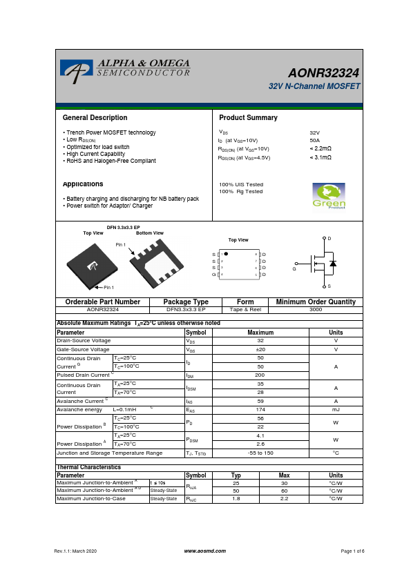
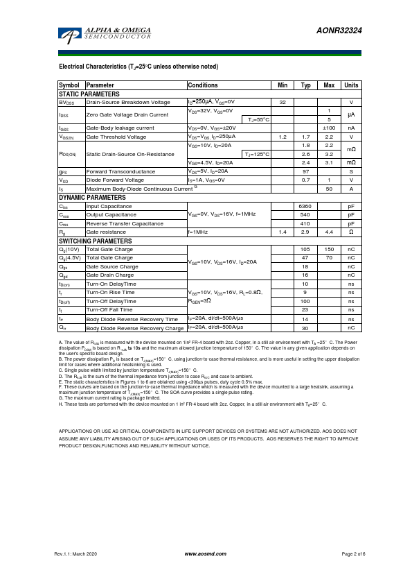
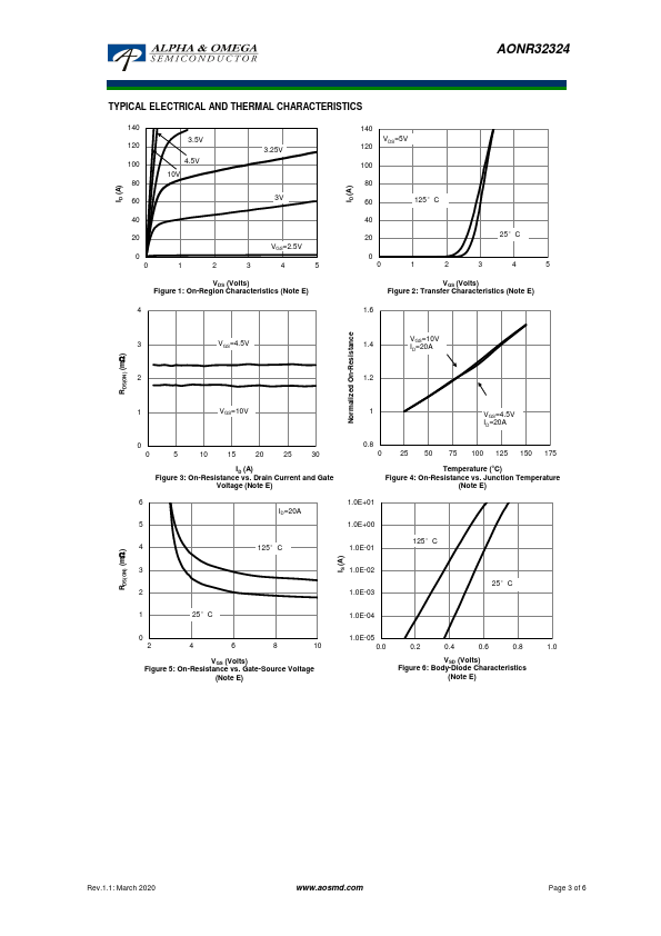
• Trench Power MOSFET technology • Low RDS(ON) • Optimized for load switch • High Current Capability • RoHS and Halogen-Free Compliant Product Summary VDS ID (at VGS=10V) RDS(ON) (at VGS=10V) RDS(ON) (at VGS=4.5V) 32V 50A < 2.2mΩ < 3.1mΩ Applications • Battery charging and discharging for NB battery pack • Power switch for Adaptor/ Charger 100% UIS Tested 100% Rg Tested DFN 3.3x3.3 EP Top View Bottom View Pin 1 Pin 1 Top View D S1 S2 S3 G4 8D 7D 6D G 5D S Orderable Part Number AONR32324 Package Type DFN3.3x3.3 EP Form Tape & Reel Minimum Order Quantity 3000 Absolute Maximum Ratings TA=25°C unless otherwise noted Parameter Symbol Drain-Source Voltage VDS Gate-Source Voltage VGS Continuous Drain Current G TC=25°C TC=100°C ID Pulsed Drain Current C IDM Continuous Drain Current TA=25°C TA=70°C IDSM Avalanche Current C IAS Avalanche energy L=0.1mH C EAS TC=25°C Power Dissipation B TC=100°C PD TA=25°C Power Dissipation A TA=70°C PDSM Junction and Storage Temperature Range TJ, TSTG Maximum 32 ±20 50 50 200 35 28 59 174 56 22 4.1 2.6 -55 to 150 Units V V A A A mJ W W °C Thermal Characteristics Parameter Symbol Typ Maximum Junction-to-Ambient A t ≤ 10s Maximum Junction-to-Ambient A D Steady-State RqJA 25 50 Maximum Junction-to-Case Steady-State RqJC 1.8 Max 30 60 2.2 Units °C/W °C/W °C/W Rev.1.1: March 2020 www.aosmd.com Page 1 of 6 AONR32324 Electrical Characteristics (TJ=25°C unless otherwise noted) Symbol Parameter Conditions Min STATIC PARAMETERS BVDSS Drain-Source Breakdown Voltage ID=250μA, VGS=0V 32 IDSS Zero Gate Voltage Drain Current VDS=32V, VGS=0V TJ=55°C IGSS Gate-Body leakage current VDS=0V, VGS=±20V VGS(th) Gate Threshold Voltage VDS=VGS, ID=250mA 1.2 VGS=10V, ID=20A RDS(ON) Static Drain-Source On-Resistance TJ=125°C VGS=4.5V, ID=20A gFS Forward Transconductance VDS=5V, ID=20A VSD Diode Forward Voltage IS=1A, VGS=0V
AONR32324 32V N-Channel MOSFET General.
| Part Number | Description |
|---|---|
| AONR32320C | 30V N-Channel MOSFET |
| AONR32314 | 30V N-Channel MOSFET |
| AONR34332C | 30V N-Channel MOSFET |
| AONR36321 | 30V N-Channel MOSFET |
| AONR36326C | 30V N-Channel MOSFET |
| AONR36329 | 30V N-Channel MOSFET |
| AONR36366 | 30V N-Channel MOSFET |
| AONR36368 | 30V N-Channel MOSFET |
| AONR21117 | 20V P-Channel MOSFET |
| AONR21305C | 30V P-Channel MOSFET |