CCSemi SI2310
N-Channel Power MOSFET
| Part No. | SI2310 |
|---|---|
| Datasheet | SI2310 Download |
| Manufacturer | CCSemi |
| Description | N-Channel Power MOSFET |
| Buy | Stock & Price |
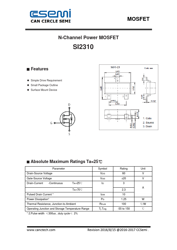
FEATURES
● Simple Drive Requirement● Small Package Outline
● Surface Mount Device
ABSOLUTE MAXIMUM RATINGS
Ta=25℃ Parameter Drain-Source Voltage Gate-Source Voltage Drain-Current -Continuous TA=25℃ TA=70℃ Pulsed Drain Current * Power Dissipation* Thermal Resistance, Junction-to-Ambient Operating Junction and Storage Temperature Range * 2.Pulse width ≤300us , duty cycle≤ 2% Symbol VDS VGS ID IDM PD RthJA Tj.Tstg Rating 60 ±20 3 2.3 10 1.25 100 -55 to 150 Unit V V A W ℃/W ℃ Revision 2016/8/15 @2016-2017 CCSemi . MOSFETELECTRICAL CHARACTERISTICS
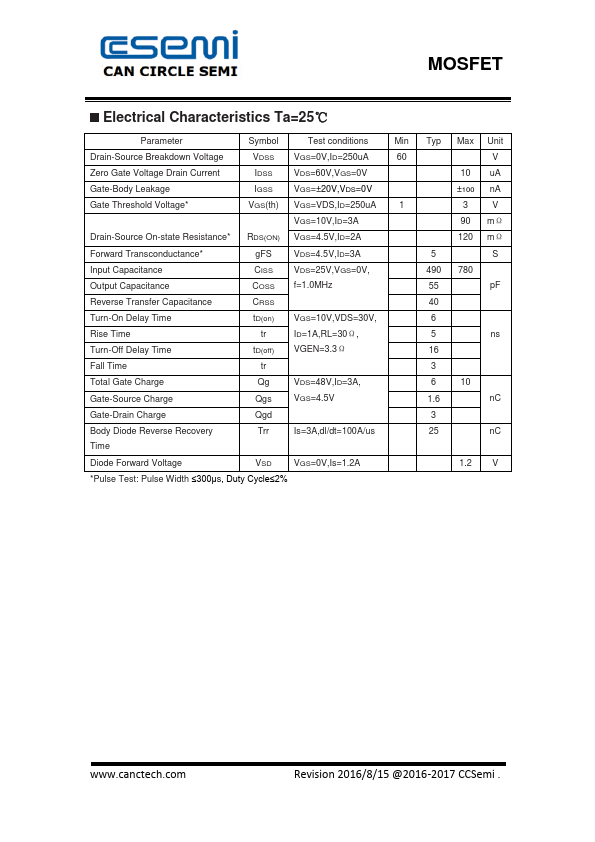
Ta=25℃ Parameter Symbol Test conditions Min Typ Max Unit Drain-Source Breakdown Voltage VDSS VGS=0V,ID=250uA 60 V Zero Gate Voltage Drain Current IDSS VDS=60V,VGS=0V 10 uA Gate-Body Leakage IGSS VGS=±20V,VDS=0V ±100 nA Gate Threshold Voltage* VGS(th) VGS=VDS,ID=250uA VGS=10V,ID=3A 1 3V 90 mΩ Drain-Source On-state Resistance* RDS(ON) VGS