FEATURES
Max rDS(on) = 24 mΩ at VGS = 10 V, ID = 7 A Max rDS(on) = 38 mΩ at VGS = 6 V, ID = 5 A Low Profile - 1 mm max in Power 33 100% UIL Tested RoHS Compliant GENERAL DESCRIPTION
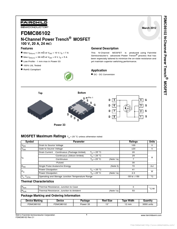
Application DC - DC Conversion Top Bottom S Pin 1 S S D G D D D D D D D 5 6 7 8 4 3 2 1 G S S S Power 33 MOSFET MAXIMUM RATINGS
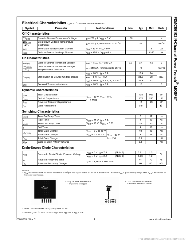
TA = 25 °C unless otherwise noted Symbol VDS VGS Parameter Drain to Source Voltage Gate to Source Voltage Drain Current -Continuous (Package limited) ID -Continuous (Silicon limited) -Continuous -Pulsed EAS PD TJ, TSTG Single Pulse Avalanche Energy Power Dissipation Power Dissipation TC = 25 °C TA = 25 °C (Note 1a) (Note 3) TC = 25 °C TC = 25 °C TA = 25 °C (Note 1a) Ratings 100 ±20 20 29 7 30 72 41 2.3 -55 to +150 mJ W °C A Units V V Operating and Storage Junction Temperature Range Thermal Characteristics RθJC RθJA Thermal Resistance, Junction to Case Thermal Resistance, Junction to Ambient (Note 1a) 3 53 °C/W Package Marking and Ordering Information Device Marking FDMC... Fairchild Semiconductor