2SJ532 Overview
Key Features
- Low on-resistance R DS(on) = 0.042 Ω typ
- Low drive current
- 4V gate drive devices
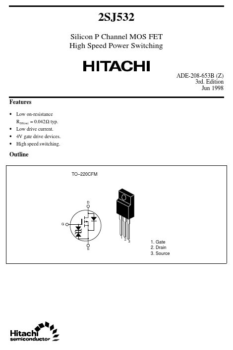
- High speed switching. Outline TO–220CFM D G 1 2 S 3
- Source 2SJ532
| Part | 2SJ532 |
|---|---|
| Description | Silicon P-Channel MOSFET |
| Category | MOSFET |
| Manufacturer | Hitachi Semiconductor |
| Size | 51.99 KB |
| Part Number | Manufacturer | Description |
|---|---|---|
| 2SJ530S | Kexin Semiconductor | Hight Speed Power Switching |
| 2SJ530S | Renesas | Silicon P-Channel MOSFET |
| 2SJ530 | Renesas | Silicon P-Channel MOSFET |
| 2SJ530S | VBsemi | 60V P-Channel MOSFET |
| 2SJ530L | Renesas | Silicon P-Channel MOSFET |