SI2301BDS
Key Features
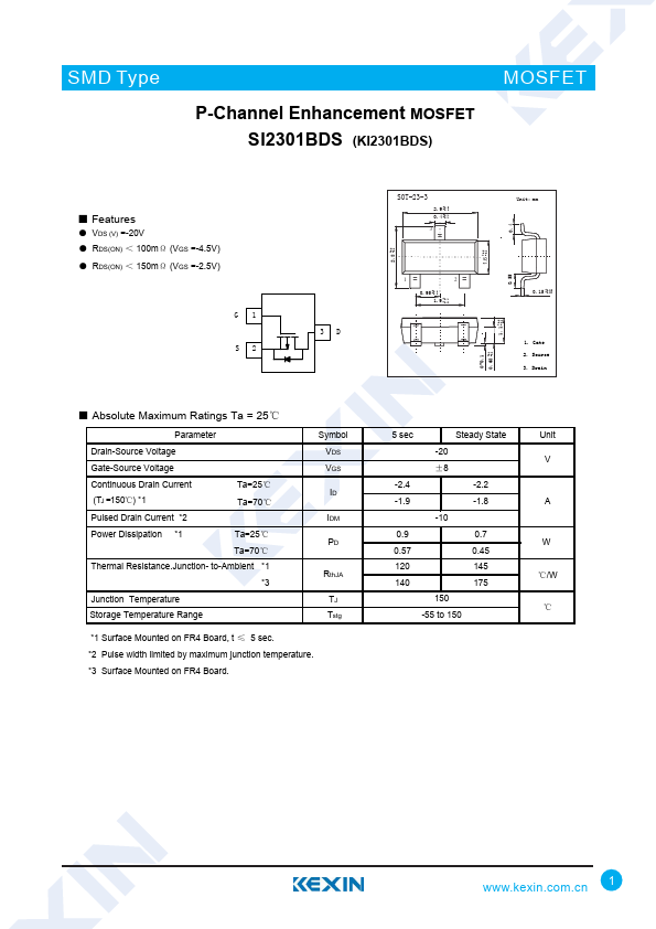
- VDS (V) =-20V
- RDS(ON) < 100mΩ (VGS =-4.5V)
- RDS(ON) < 150mΩ (VGS =-2.5V) G1 S2 3D
| Part Number | Manufacturer | Description |
|---|---|---|
| SI2301BDS-T1-GE3 | VBsemi | P-Channel MOSFET |
| SI2301BDS | SiPU | P-Channel Enhancement Mode Field Effect Transistor |
| SI2301B | UMW | P-Channel MOSFET |
| SI2301ADS | Vishay | P-Channel MOSFET |
| SI2301A | Micro Commercial Components | P-Channel MOSFET |
| SI2301DS-T1-GE3 | VBsemi | P-Channel MOSFET |
| SI2301 | YANGJING | P-Channel MOSFET |
| SI2301CDS | Vishay | P-Channel MOSFET |
| Si2301 | SiPU | P-Channel MOSFET |
| Si2301DS | TEMIC Semiconductors | P-Channel MOSFET |