BS107A
Features
- AEC- Q101 Qualified and PPAP Capable
- This is a Pb- Free Device-
MAXIMUM RATINGS Rating
Symbol Value Unit
Drain
- Source Voltage
Gate- Source Voltage
- Continuous
- Non- repetitive (tp ≤ 50 ms)
Drain Current Continuous (Note 1) Pulsed (Note 2)
Total Device Dissipation @ TA = 25°C Derate above 25°C
VGS VGSM
ID IDM PD
Vdc
± 20
Vdc
± 30
Vpk m Adc 250 500
350 m W
Operating and Storage Junction Temperature Range
TJ, Tstg
- 55 to
°C
Stresses exceeding those listed in the Maximum Ratings table may damage the device. If any of these limits are exceeded, device functionality should not be assumed, damage may occur and reliability may be affected. 1. The Power Dissipation of the package may result in a lower continuous drain current. 2. Pulse Test: Pulse Width v 300 ms, Duty Cycle v 2.0%. http://onsemi.
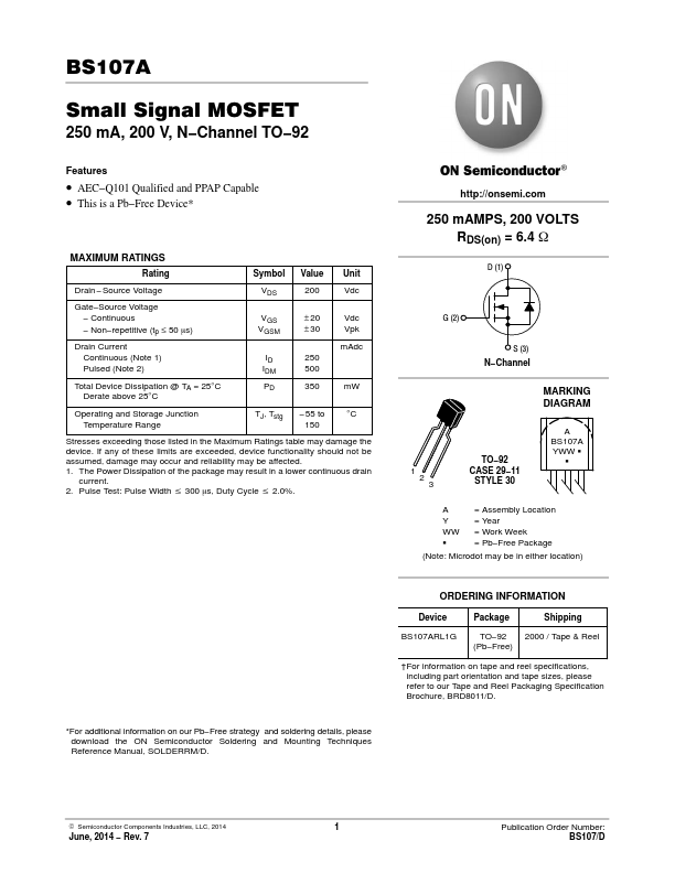
250 m AMPS, 200 VOLTS RDS(on) = 6.4 W
D (1)
G (2)
S (3) N- Channel
MARKING DIAGRAM
1 2 3
TO- 92 CASE 29- 11
STYLE 30
A BS107A YWW G
= Assembly...