PLL205-54
PLL205-54 is manufactured by PhaseLink.
m Preliminary PLL205-54 o c . Programmable Clock Generator for VIA KT-266 Chipset U 4 t Features
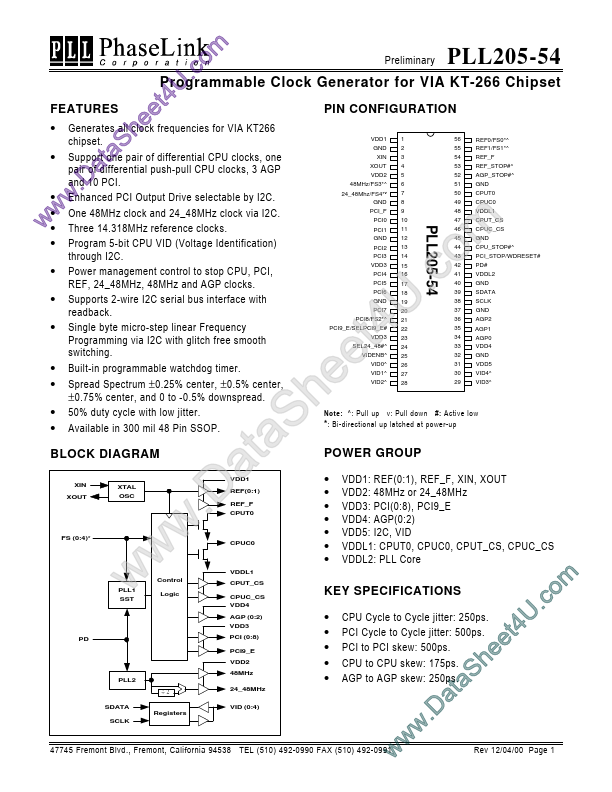
PIN CONFIGURATION e e
- Generates all clock frequencies for VIA KT266 h chipset. S a
- Support one t pair of differential CPU clocks, one pair of a differential push-pull CPU clocks, 3 AGP and 10 PCI. D .
- w Enhanced PCI Output Drive selectable by I2C.
- w One 48MHz clock and 24_48MHz clock via I2C. w- Three 14.318MHz reference clocks.
VDD1 GND 1 2 3 4 5 6 7 8 9 56 55 54 53 52 51 50 49 48 47 46 45 44 43 42 41 40 39 38 37 36 35 34 33 32 31 30 29 REF0/FS0- ^ REF1/FS1- ^ XIN XOUT REF_F REF_STOP#^ VDD2 48MHz/FS3- ^ AGP_STOP#^ GND CPUT0 CPUC0
- -
- -
- -
- -
Program 5-bit CPU VID (Voltage...