STMicroelectronics 2N6668
SILICON PNP POWER DARLINGTON TRANSISTOR
| Part No. | 2N6668 |
|---|---|
| Datasheet | 2N6668 Download |
| Manufacturer |  STMicroelectronics |
| Description | SILICON PNP POWER DARLINGTON TRANSISTOR |
| Buy | Stock & Price |
APPLICATIONS
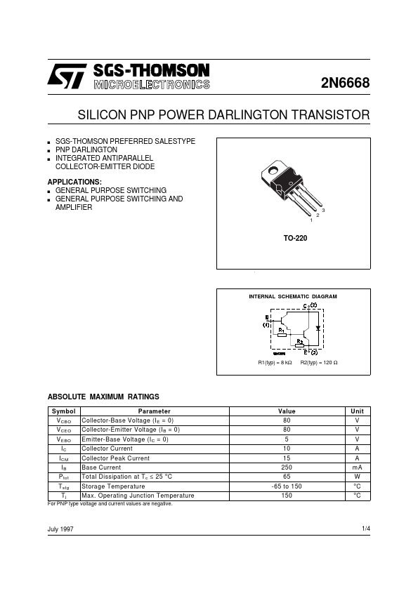
: GENERAL PURPOSE SWITCHING s GENERAL PURPOSE SWITCHING AND AMPLIFIER s 3 1 2 TO-220 INTERNAL SCHEMATIC DIAGRAM R1(typ) = 8 kΩ R2(typ) = 120 ΩABSOLUTE MAXIMUM RATINGS
Symbol V CBO V CEO V EBO IC I CM IB P tot T stg Tj Parameter Collector-Base Voltage (I E = 0) Collector-Emitter Voltage (I B = 0) Emitter-Base Voltage (I C = 0) Collector Current Collector Peak Current Base Current Total Dissipation at T c ≤ 25 o C Storage Temperature Max. Operating Junction Temperature Value 80 80 5 10 15 250 65 -65 to 150 150 Unit V V V A A mA W o o C C For PNP type voltage and current values are negative. July 1997 1/4 2N6668 THERMAL DATA R thj-case R thj-amb Thermal Resistance Junction-case Thermal Resistance Junction-ambient Max Max 1.92 62.5 o o C/W C/WELECTRICAL CHARACTERISTICS
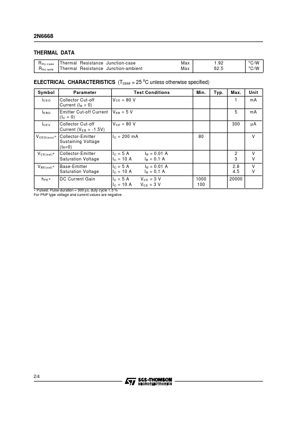
(Tcase = 25 oC unless otherwise specified) Symbol I CEO I EBO I CEV Parameter Collector Cut-off Current (I B = 0) Emitter Cut-off Current (I C = 0) Collector Cut-off Current (V EB = -1.5V) Test Conditions V CE = 80 V V EB = 5 V V CE = 80 V I C = 200 mA 80 Min.