NAND512-A
Overview
- HIGH DENSITY NAND FLASH MEMORIES - Up to 1 Gbit memory array - Up to 32 Mbit spare area - Cost effective solutions for mass storage applications NAND INTERFACE - x8 or x16 bus width - Multiplexed Address/ Data - Pinout compatibility for all densities SUPPLY VOLTAGE - 1.8V device: VDD = 1.7 to 1.95V - 3.0V device: VDD = 2.7 to 3.6V PAGE SIZE - x8 device: (512 + 16 spare) Bytes - x16 device: (256 + 8 spare) Words BLOCK SIZE - x8 device: (16K + 512 spare) Bytes - x16 device: (8K + 256 spare) Words PAGE READ / PROGRAM - Random access: 12µs (max) - Sequential access: 50ns (min) - Page program time: 200µs (typ) COPY BACK PROGRAM MODE - Fast page copy without external buffering FAST BLOCK ERASE - Block erase time: 2ms (Typ) STATUS REGISTER ELECTRONIC SIGNATURE CHIP ENABLE ‘DON’T CARE’ OPTION - Simple interface with microcontroller SERIAL NUMBER OPTION HARDWARE DATA PROTECTION - Program/Erase locked during Power transitions Figure
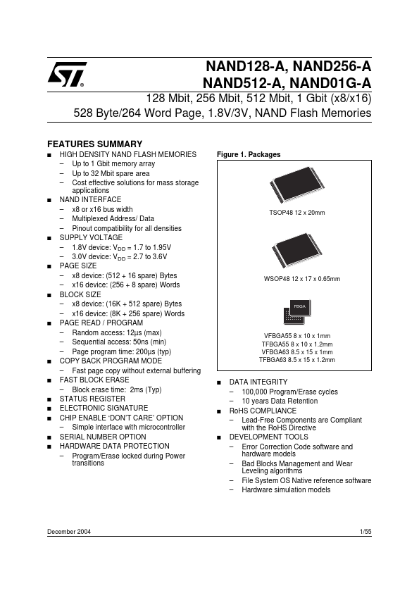
- Packages