2SC3352
Overview
SavantIC Semiconductor Product Specification Silicon NPN Power Transistors 2SC3352 DESCRIPTION ·With TO-220Fa package ·High voltage ·High speed switching APPLICATIONS ·For high speed switching ap...
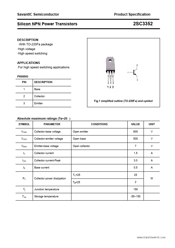
SavantIC Semiconductor Product Specification Silicon NPN Power Transistors 2SC3352 DESCRIPTION ·With TO-220Fa package ·High voltage ·High speed switching APPLICATIONS ·For high speed switching ap...