Datasheet Details
| Part number | AO4832 |
|---|---|
| Manufacturer | Alpha & Omega Semiconductors |
| File Size | 314.22 KB |
| Description | 30V Dual N-Channel MOSFET |
| Download | AO4832 Download (PDF) |
|
|
| Part number | AO4832 |
|---|---|
| Manufacturer | Alpha & Omega Semiconductors |
| File Size | 314.22 KB |
| Description | 30V Dual N-Channel MOSFET |
| Download | AO4832 Download (PDF) |
|
|
|
The AO4832 uses advanced trench technology to provide excellent RDS(ON) with low gate charge.
This device is suitable for high side switch in SMPS and general purpose applications.
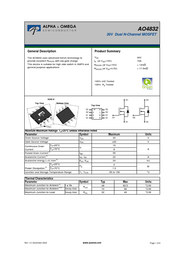
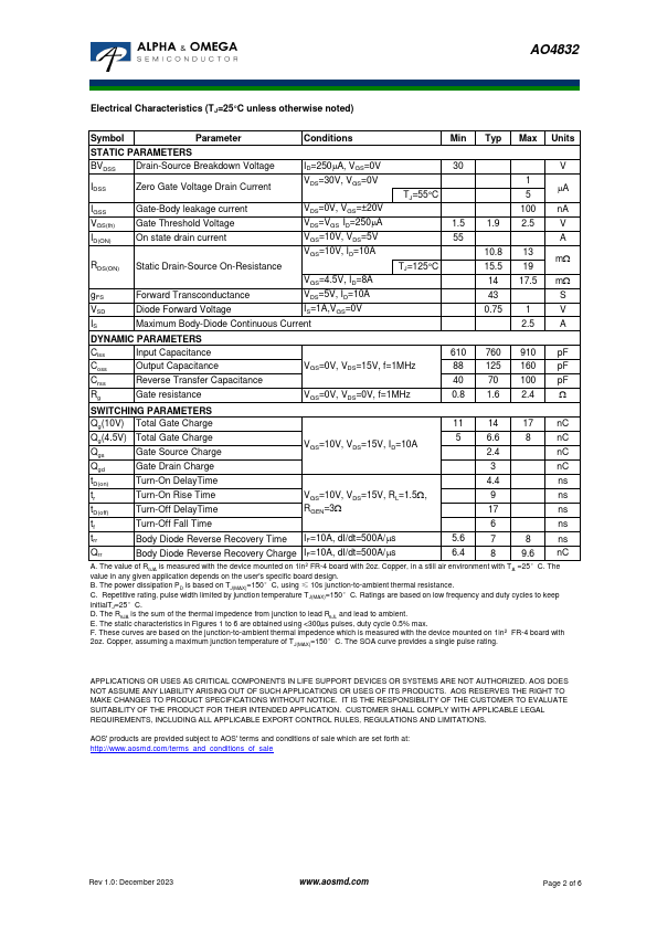
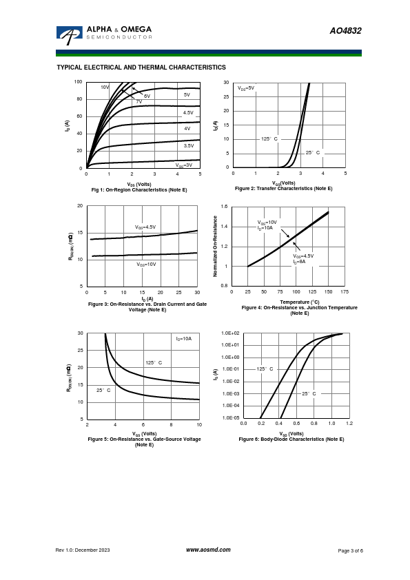
Product Summary VDS ID (at VGS=10V) RDS(ON) (at VGS=10V) RDS(ON) (at VGS=4.5V) 100% UIS Tested 100% Rg Tested 30V 10A < 13mW < 17.5mW Top View SOIC-8 Bottom View Top View S2 1 8 G2 2 7 S1 3 6 G1 4 5 D2 D2 D1 D1 G1 Pin1 Absolute Maximum Ratings TA=25°C unless otherwise noted Parameter Symbol Drain-Source Voltage VDS Gate-Source Voltage VGS Continuous Drain TA=25°C Current TA=70°C Pulsed Drain Current C Avalanche Current C Avalanche energy L=0.1mH C ID IDM IAS, IAR EAS, EAR TA=25°C Power Dissipation B TA=70°C PD Junction and Storage Temperature Range TJ, TSTG Maximum 30 ±20 10 8 55 22 24 2 1.3 -55 to 150 D1 G2 S1 Thermal Characteristics Parameter Symbol Typ Maximum Junction-to-Ambient A t ≤ 10s Maximum Junction-to-Ambient A D Steady-State RqJA 48 74 Maximum Junction-to-Lead Steady-State RqJL 32 Max 62.5 90 40 D2 S2 Units V V A A mJ W °C Units °C/W °C/W °C/W Rev 1.0: December 2023 www.aosmd.com Page 1 of 6 AO4832 Electrical Characteristics (TJ=25°C unless otherwise noted) Symbol Parameter Conditions Min Typ Max Units STATIC PARAMETERS BVDSS Drain-Source Breakdown Voltage ID=250mA, VGS=0V 30 V IDSS Zero Gate Voltage Drain Current VDS=30V, VGS=0V TJ=55°C 1 mA 5 IGSS Gate-Body leakage current VDS=0V, VGS=±20V 100 nA VGS(th) Gate Threshold Voltage VDS=VGS ID=250mA 1.5 1.9 2.5 V ID(ON) On state drain current VGS=10V, VDS=5V 55 A RDS(ON) Static Drain-Source On-Resistance VGS=10V, ID=10A TJ=125°C 10.8 13 mW 15.5 19 VGS=4.5V, ID=8A 14 17.5 mW gFS Forward Transconductance VDS=5V, ID=10A 43 S VSD Diode Forward Voltage IS=1A,VGS=0V 0.75 1 V IS Maximum Body-Diode Continuous Current 2.5 A DYNAMIC PARAMETERS Ciss Input Capacitance Coss Output Capa
AO4832 30V Dual N-Channel MOSFET General.
| Brand Logo | Part Number | Description | Manufacturer |
|---|---|---|---|
| AO4832 | Dual N-Channel MOSFET | Kexin | |
| AO4832 | 30V Dual N-Channel MOSFET | VBsemi | |
| EVVOSEMI | AO4832 | 30V Dual N-Channel MOSFET | EVVOSEMI |
| UMW | AO4832 | 30V Dual N-Channel MOSFET | UMW |
| Part Number | Description |
|---|---|
| AO4830 | 80V Dual N-Channel MOSFET |
| AO4836 | Dual N-Channel MOSFET |
| AO4838 | 30V Dual N-Channel MOSFET |
| AO4800 | 30V Dual N-Channel MOSFET |
| AO4800B | 30V Dual N-Channel MOSFET |
| AO4800BL | Dual N-Channel MOSFET |
| AO4801 | Dual P-Channel MOSFET |
| AO4801A | 30V P-Channel MOSFET |
| AO4802 | Dual N-Channel MOSFET |
| AO4802L | Dual N-Channel MOSFET |